RF Filter Design for ESP32-S3, Part 2: PCB Effects and EM Co-Simulation
An ideal RF filter changes once PCB geometry is included. Part 2 imports the Altium layout into CST, uses EM co-simulation to expose trace, pad, and coupling parasitics, and re-optimizes the component values to restore the target S₁₁ response.

This is Part 2 of a three-part series on ESP32-S3 RF filter design.
Inclusion of PCB physical effects and intermediate validation
"This velocity is so nearly that of light, that it seems we have strong reason to conclude that light itself is an electromagnetic disturbance in the form of waves propagated through the electromagnetic field according to electromagnetic laws."
— James Clerk Maxwell, Lecture at King's College, London (1862)
Introduction
The first stage of this workflow established a clean electrical baseline: an ideal CLC filter, optimized in the schematic domain, transferred to Altium as a first PCB implementation. At that stage, the circuit existed in two parallel representations, a mathematically refined schematic in CST and a physical layout in Altium, but these two representations had never been connected. The simulation had no knowledge of the board.
This second stage closes that gap. By exporting the PCB layout from Altium and importing it directly into CST Studio Suite, the physical structure of the board becomes part of the electromagnetic model. The routing geometry, pad shapes, copper transitions, and dielectric stack all begin to influence the simulated response. The filter is still built from ideal lumped components, but the environment in which those components operate is no longer ideal.
The result is a co-simulation: the circuit elements are evaluated together with the electromagnetic behavior of the layout, producing a response that reflects not just the component values but also the parasitic effects introduced by the PCB itself. This is the first stage at which the simulation can reveal problems that no schematic-level analysis can detect, frequency shifts, impedance distortions, and coupling paths that exist only because of physical geometry.
This article documents that transition, from the export of the Altium layout to the re-optimization of component values under layout-aware conditions, and closes with a direct comparison against the Stage 1 baseline.
Export from Altium
The first step is to generate the ODB++ output from the Altium Designer project. ODB++ is a manufacturing exchange format that captures the complete PCB structure, layer stackup, copper geometry, pad definitions, drill data, and component placement, in a form that CST Studio Suite can interpret directly as a three-dimensional electromagnetic model.
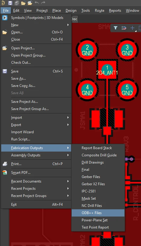
In Altium Designer, go to File → Fabrication Outputs → ODB++ Files. In the output configuration dialog, verify that all signal layers, the board outline, and the component placement data are included in the export. Confirm the stackup parameters are correctly defined, layer thicknesses, dielectric constants, and copper weights, since these values will directly determine how CST constructs the 3D model.
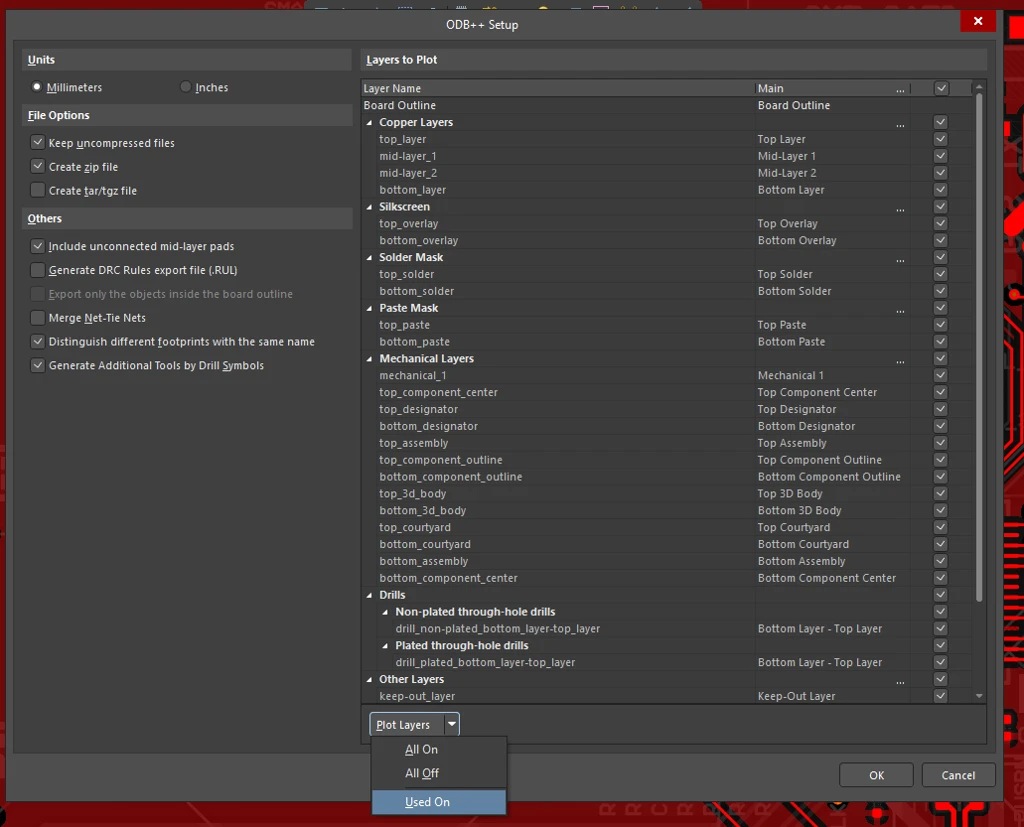
Don’t forget to check “Used On” to plot all used layers.
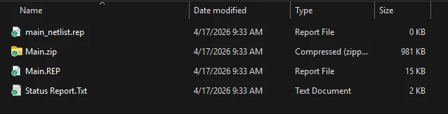
Generate the output and confirm that the ODB++ package has been created without errors before proceeding to the import step. All files will be present at the Project Outputs folder.
Import into CST Studio Suite
With the ODB++ file available, the next step is to load the PCB layout into CST Studio Suite as a three-dimensional structure.
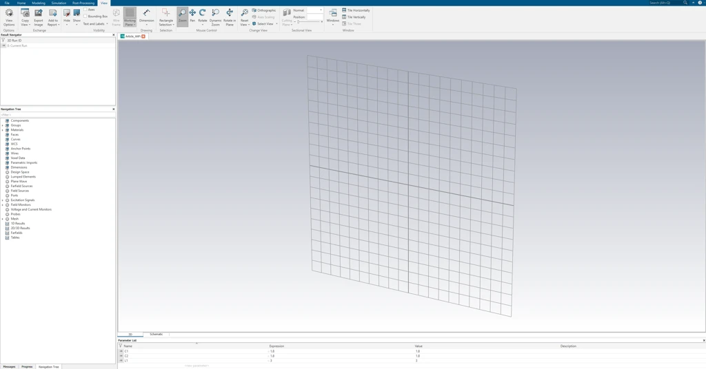
Load the 3D layout
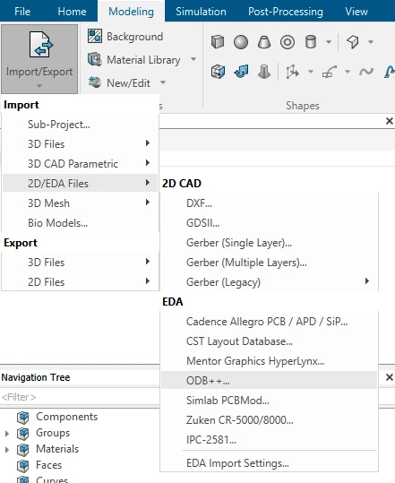
In CST, go to Modeling → Import/Export → 2D/EDA Files → ODB++ and select the exported package.
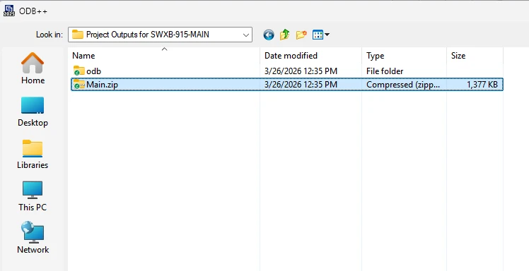
CST will parse the file and reconstruct the board geometry, including all copper layers, dielectric substrates, and component footprints, as a full 3D model. Review the imported structure carefully to confirm that the layer stack, copper features, and board outline match the original Altium design.
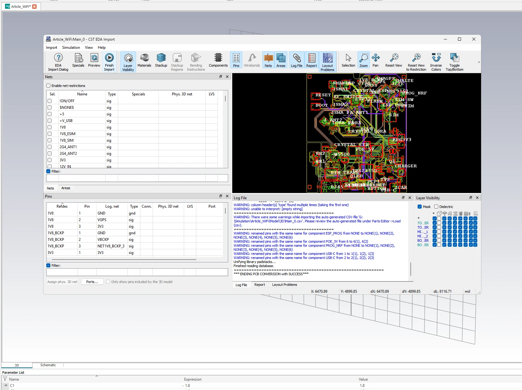
You have now successfully imported the board from Altium.
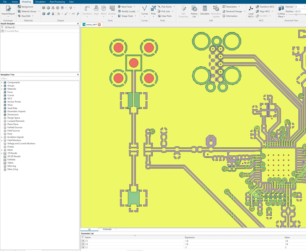
3D Model Trimming
The imported model represents the complete ESP32-S3 PCB, which is far larger than the region relevant to the filter simulation. Working with the full board geometry at this stage is unnecessary and would increase simulation time and RAM usage without adding meaningful information to the filter analysis. The model must therefore be trimmed to isolate only the region of interest before any further setup is performed.
Region of interest.
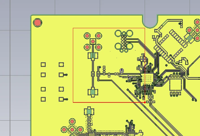
In the CST 3D editor, use the geometry cutting tools to remove all areas of the board outside the filter region. The area to retain is the CLC network itself, components CRF1, R0L, and CRF2, together with their immediate copper connections: the RF trace entering the filter from the ESP32-S3 RF port, the trace exiting toward the antenna matching network, and the ground return paths directly associated with the shunt capacitor pads. Copper and dielectric geometry beyond this boundary does not contribute meaningfully to the filter response and should be excluded.
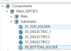
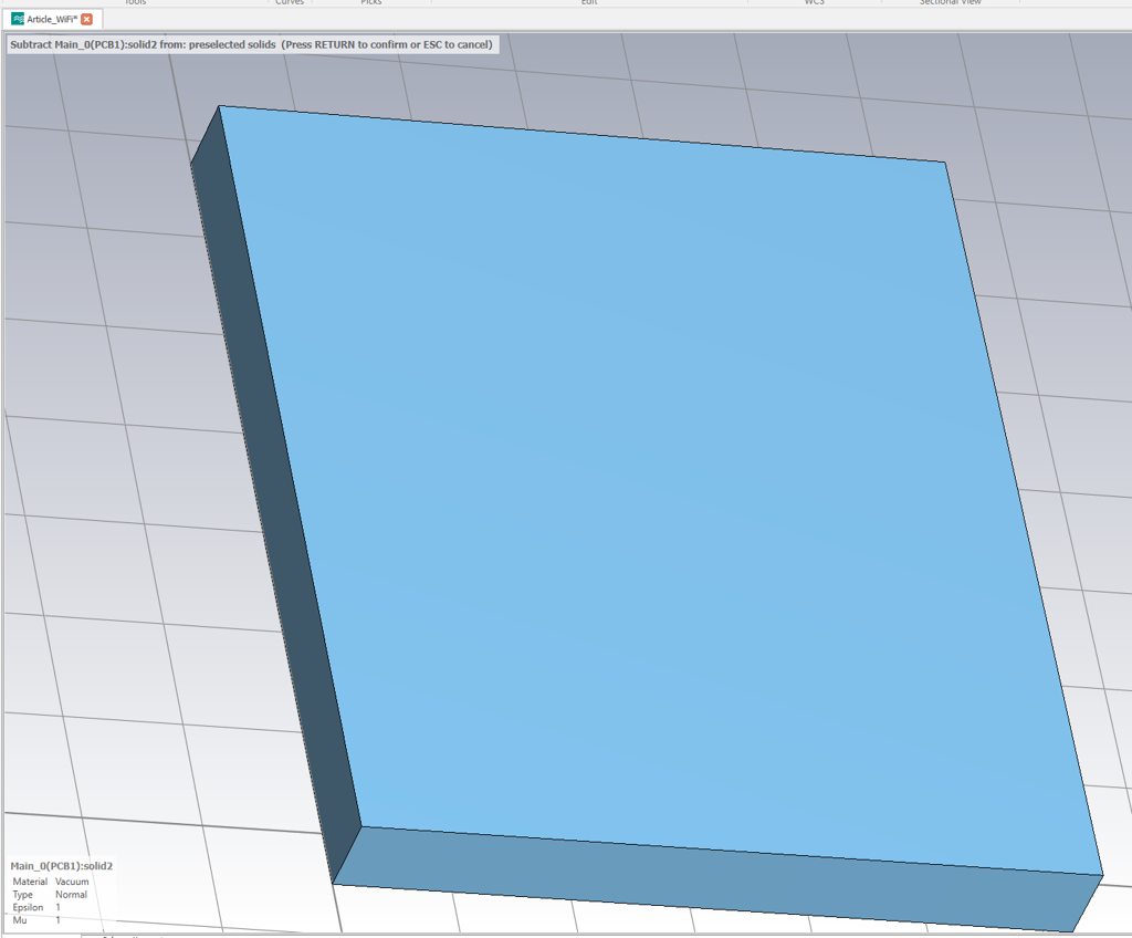
Delete the top and bottom solders.
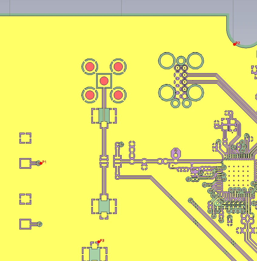
Press “P” to select points around and below the desired geometry.
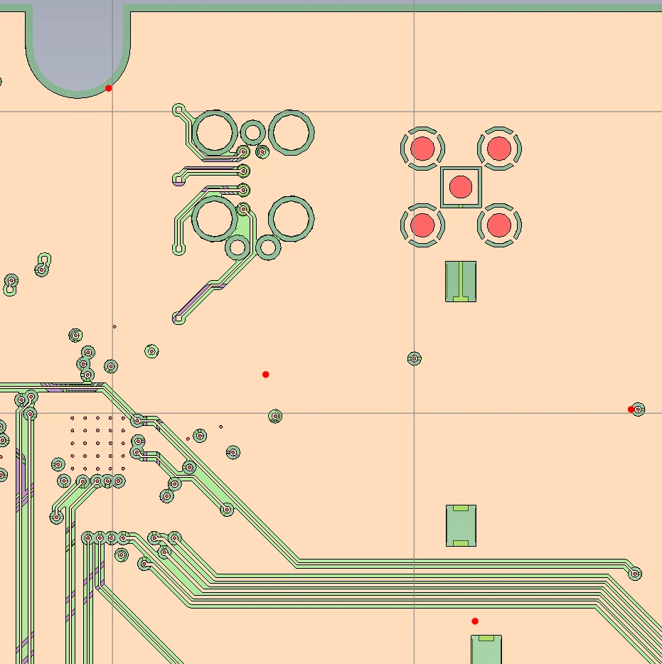
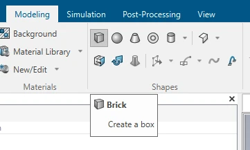
Click on Modeling - Shapes - Brick, press ESC to automatically select the points.
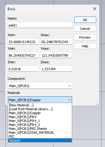
In the Brick dialog box, select the material Vacuum and press OK.
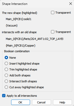
A new dialog box will appear, Shape Intersection, select None in Boolean combination and check “Apply to all intersections” and click OK.
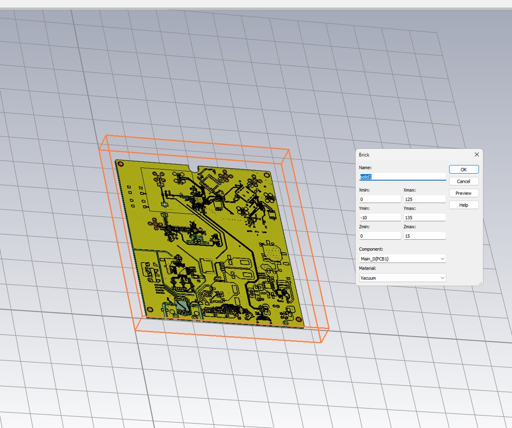
Click on Brick again and select around your entire board, same process as the first.
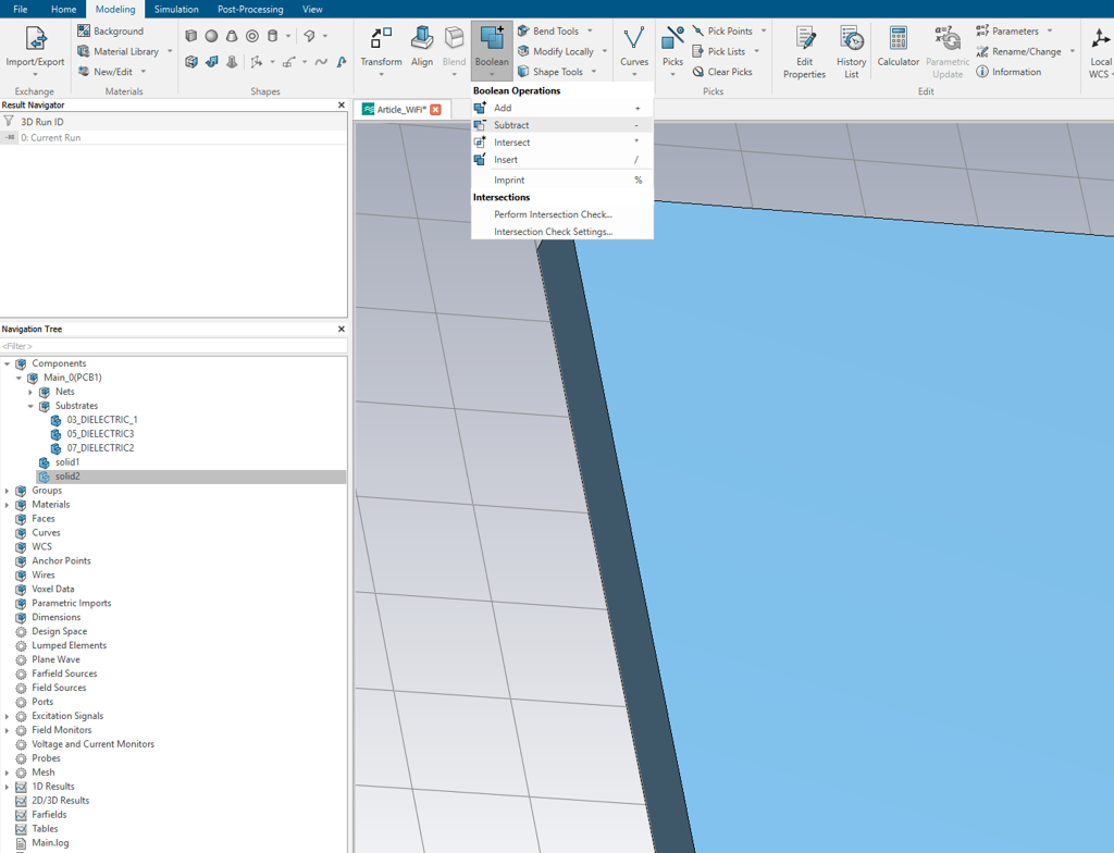
Select your second Brick and in the Modeling - Tools - Boolean, select Subtract or press “-” (minus).
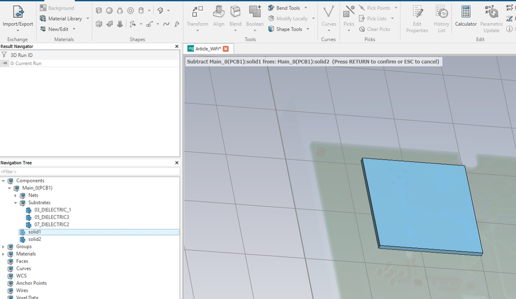
Double-click on the first Brick to select it and press ENTER.
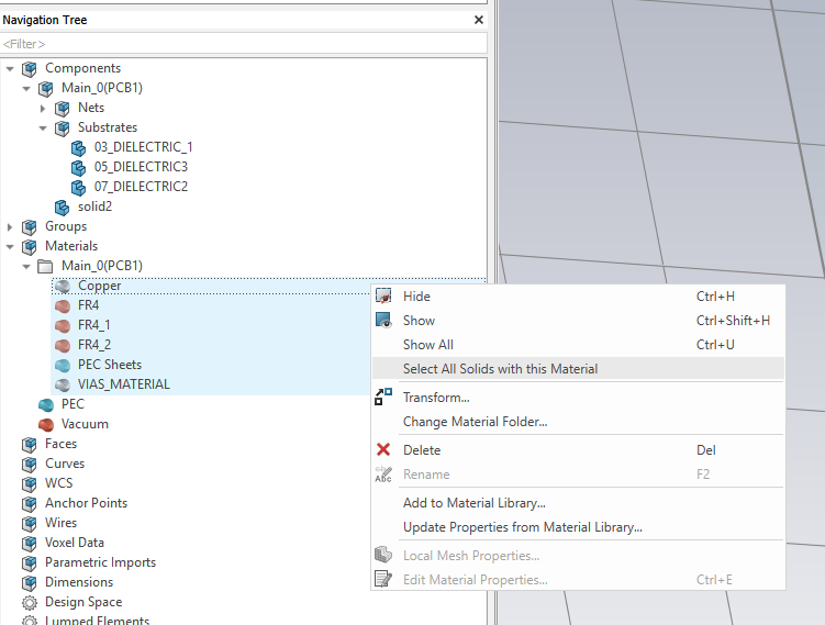
In Navigation Tree - Materials, select all imported materials and with the right-click choose the option “Select All Solids with this Material”.
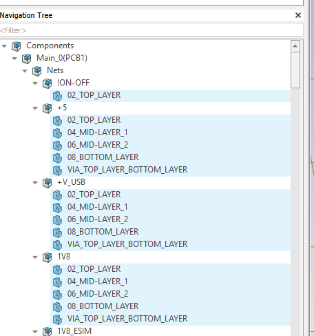
All traces will be selected.
With them selected, click “-” again and select your resulting Brick, after this press ENTER.
The resulting trimmed 3D objects.
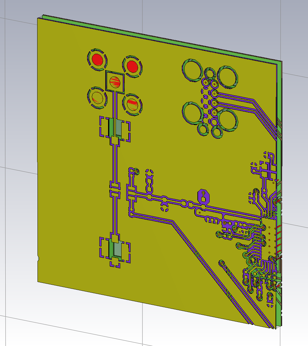
After trimming, review the resulting structure to confirm that no relevant copper feature has been inadvertently removed. The cut boundaries should fall on electrically neutral regions, away from pads, vias, and trace bends, to avoid introducing artificial discontinuities into the model.
Define the RF ports
After the import is complete, the RF ports must be defined. These ports establish the excitation and termination points of the filter path within the 3D model and must correspond to the same network entry and exit points used in the Stage 1 schematic simulation. Correct port placement is essential, misaligned ports will produce results that cannot be meaningfully compared against the Stage 1 baseline.
Next, define the component connection points on the layout. These are the locations where the ideal lumped elements will be connected to the physical model during co-simulation. Each connection point must be mapped to the corresponding pads of the filter components, CRF1, R0L, and CRF2, as placed in the Altium schematic. This step is what allows the co-simulation to treat the physical layout and the circuit elements as a single integrated model.
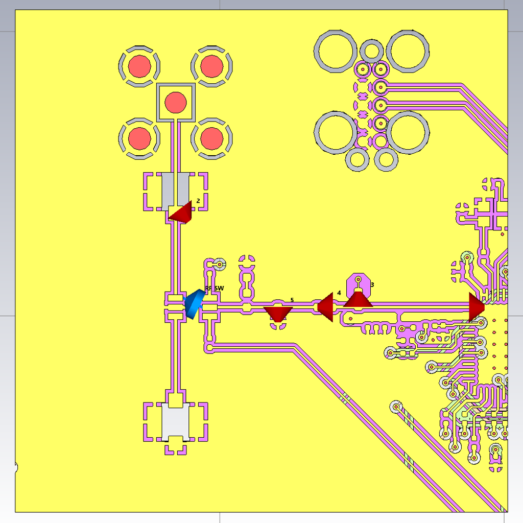
Navigate to the RF output pin.
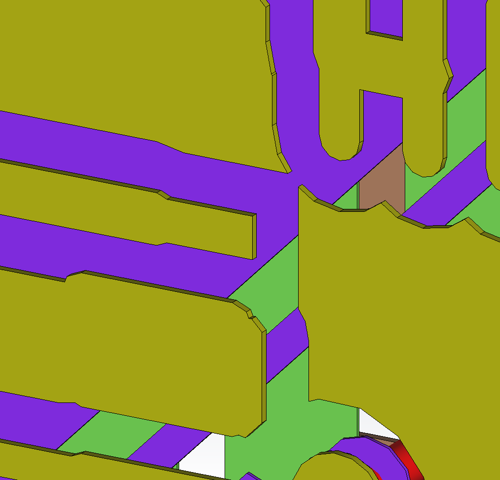
Press “S” to select the edges, RF pin and ground
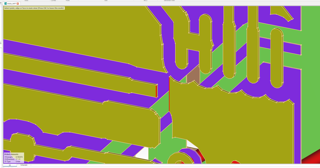
In tab Simulation, select Discrete Port in Sources and Loads.
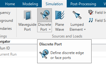
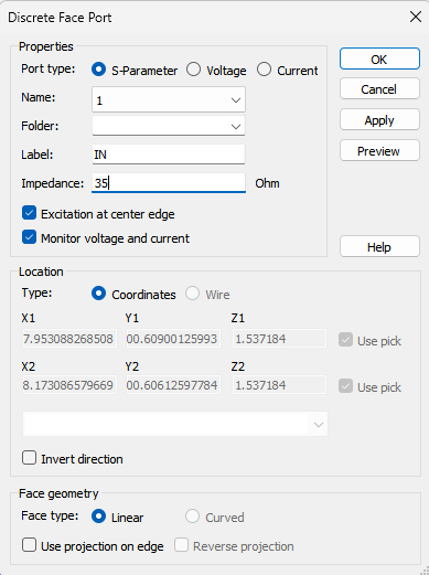
For the dialog window, set the name (I prefer “IN”) and set the impedance to 35 Ohms as mentioned by Espressif documentation.
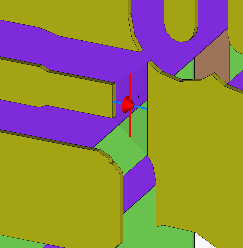
Now you have an input port.
Repeat it for the Output (OUT) and the components (CRF1, R0L and CRF2), all with 50 Ohms.
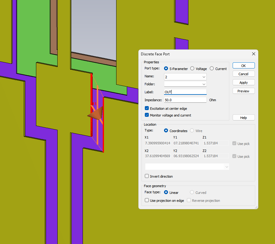
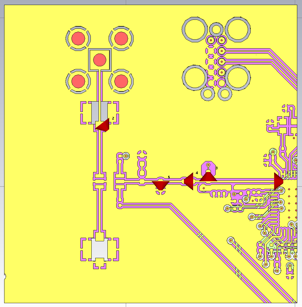
You have now all the ports needed. The next step is adding the RF Switch.
First, add a Copper brick for each pin used with 0.1mm of height.
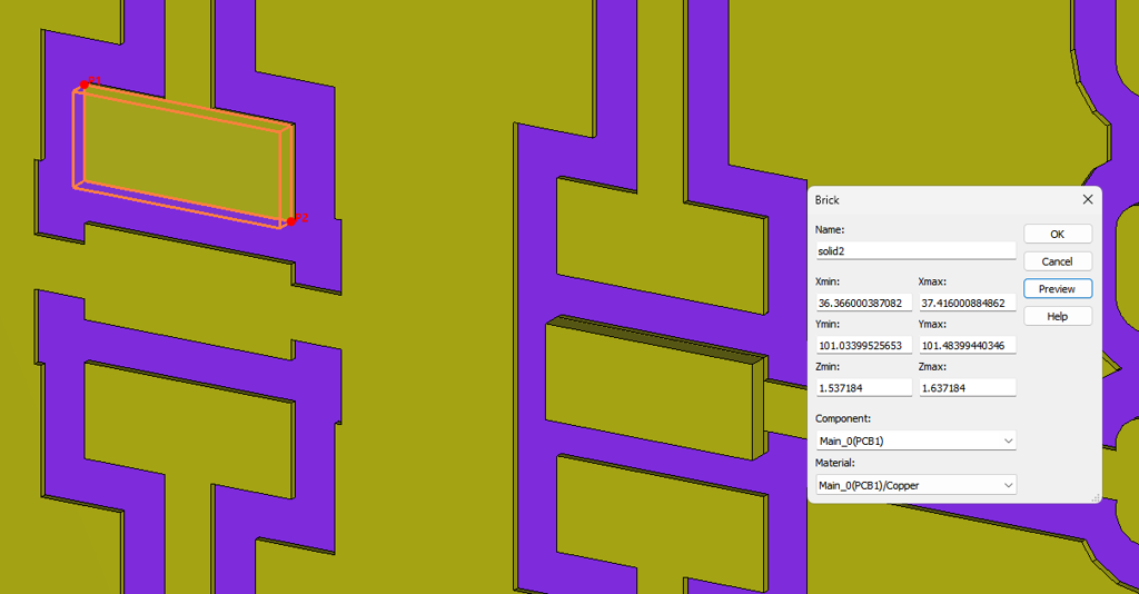
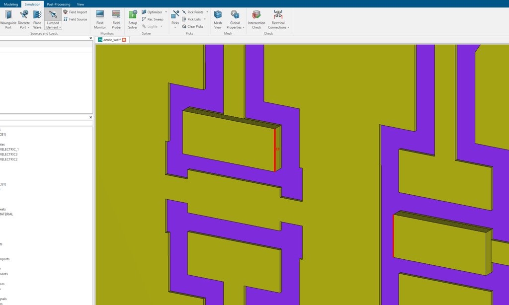
Select the edges that connect them and add a lumped element from tab Simulation - Sources and Loads.
Set the name and choose the Type Touchstone.
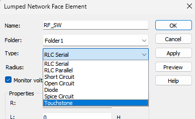
In the properties, click on Circuit File.
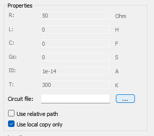
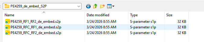
Since I’m using the PE4259 RF-Switch from Psemi, they source the models from the component, I’ll use the RFC to RF1, since I’m modeling from the common pin to pin 1.
Click on OK and you will have completed the components.
Circuit and EM Co-Simulation
With the 3D layout imported and the connection points defined, the co-simulation can be configured. At this stage, the lumped components remain ideal, the same C1, C2, and L1 values obtained from the Stage 1 optimization, but they now operate within the electromagnetic environment of the physical board rather than in an abstract schematic domain.
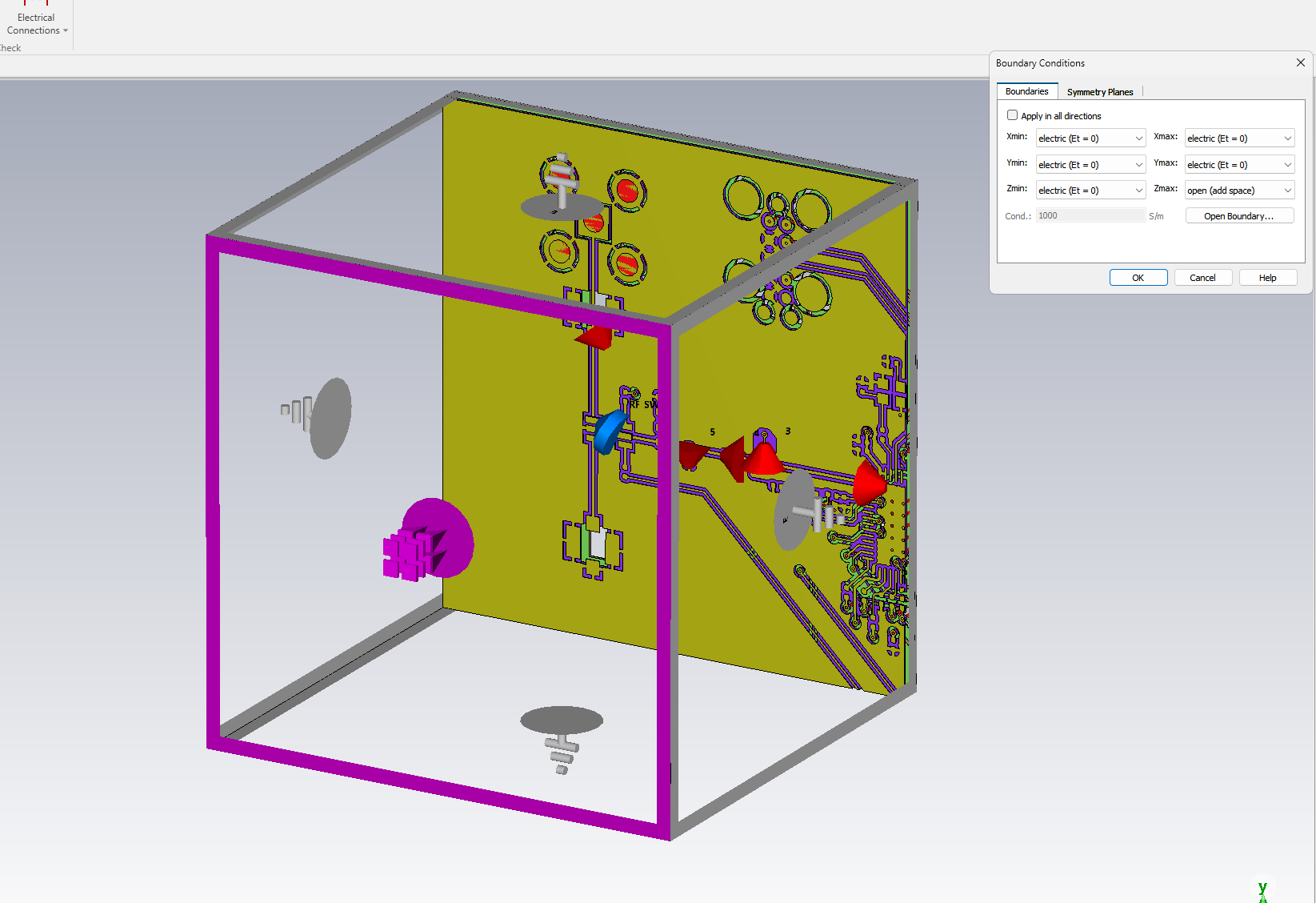
in 3D tab, select Simulation - Boundaries.
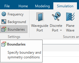
Set Zmax to open (add space).
You can now start the simulation in Home - Start Simulation.
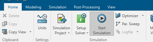
The time it needs to simulate depends on your project size, complexity and computer specs.
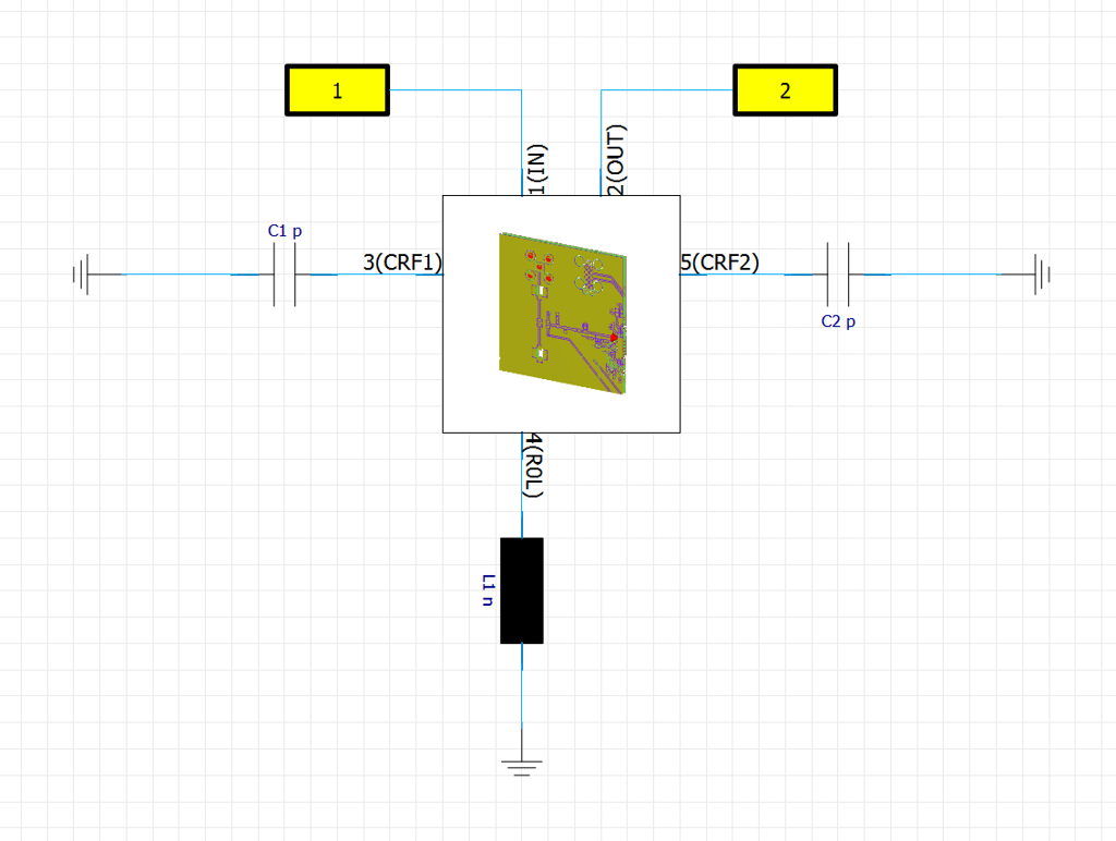
In the Schematic tab, right-click the block containing the ports connected to the 3D and select “Change Pin Layout”.
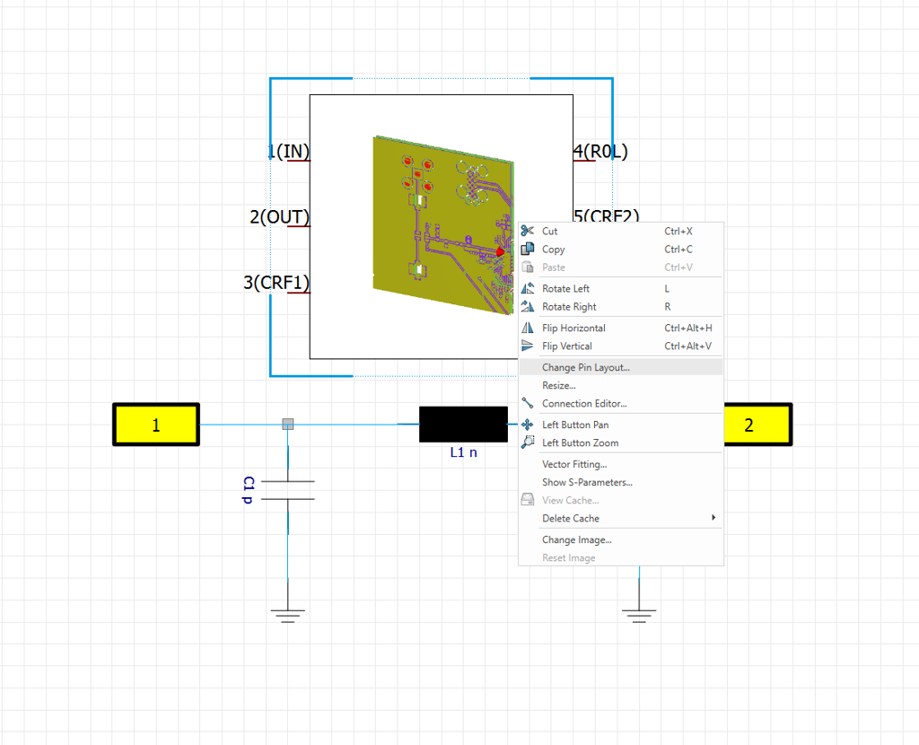
Rearrange them as you like; I personally prefer them this way, as shown in the next image.
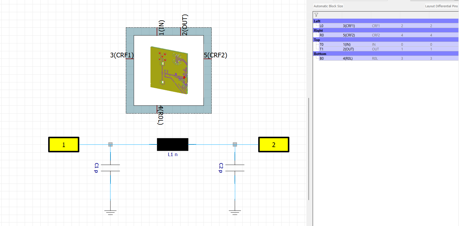
Press ESC and disconnect all components.
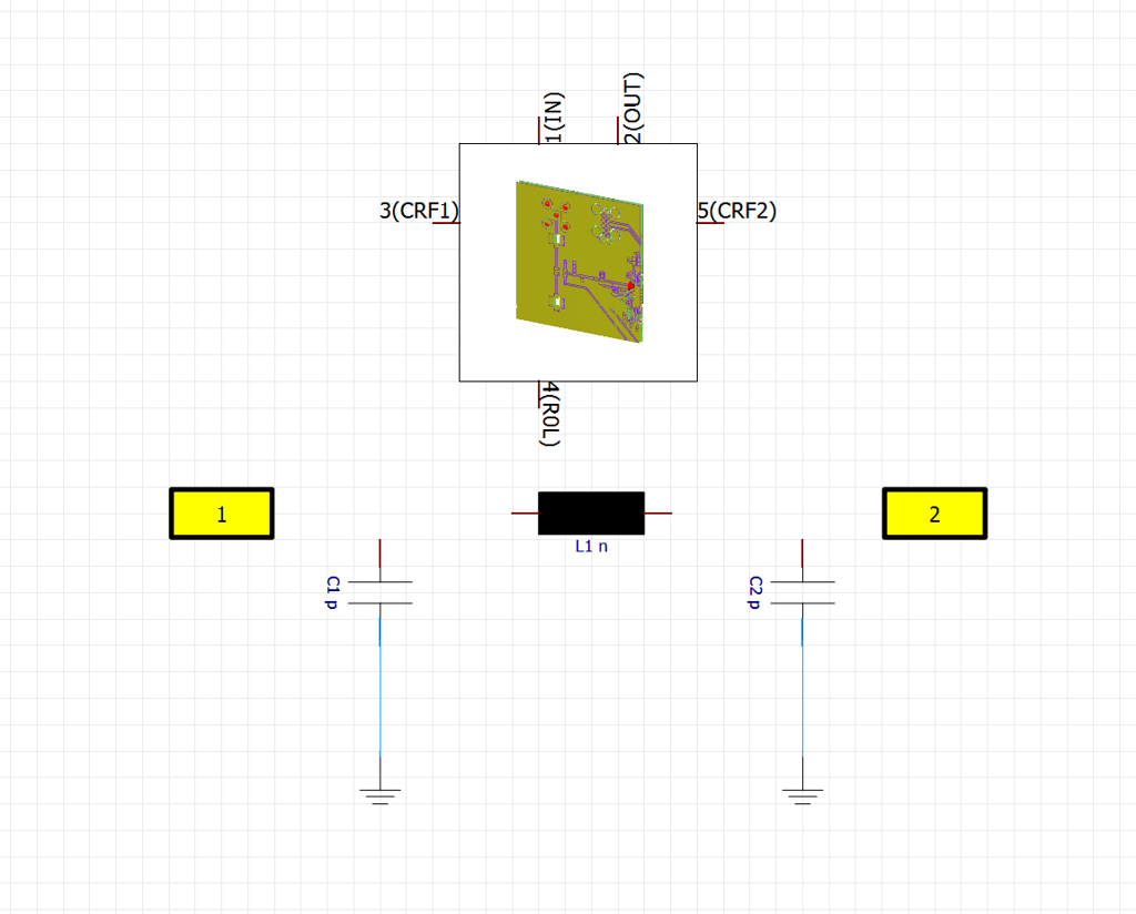
Connect the ports 1 - 1 and 2 - 2. Connect the components' one pin to the port and the other to ground.
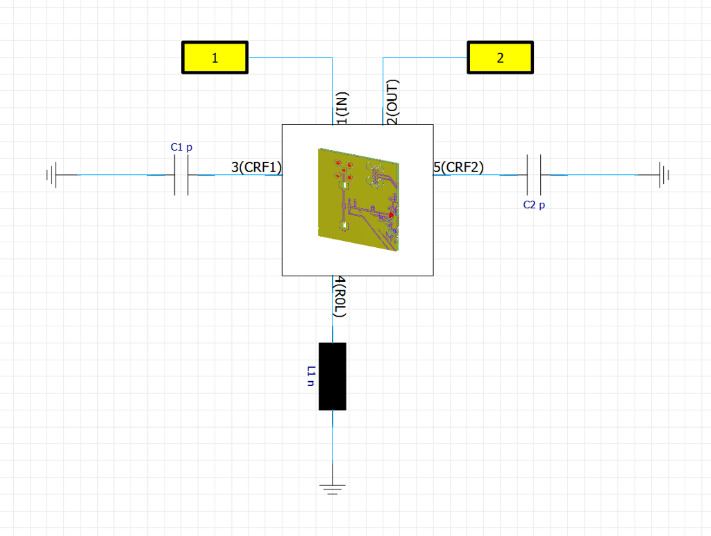
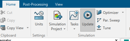
With the 3D simulation complete and the circuit schematic connected, click on Home - Update, the simulation here is very fast compared to the 3D.
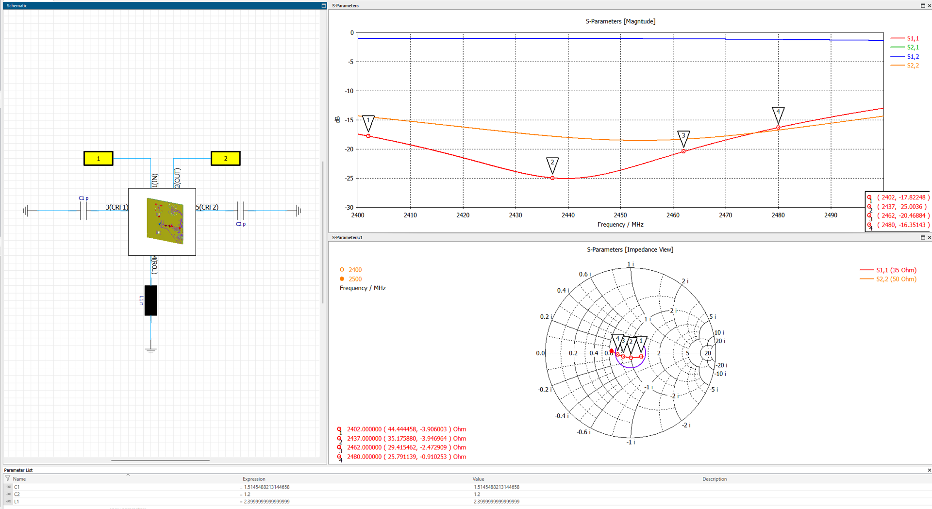
Check the S-parameters, it has changed.
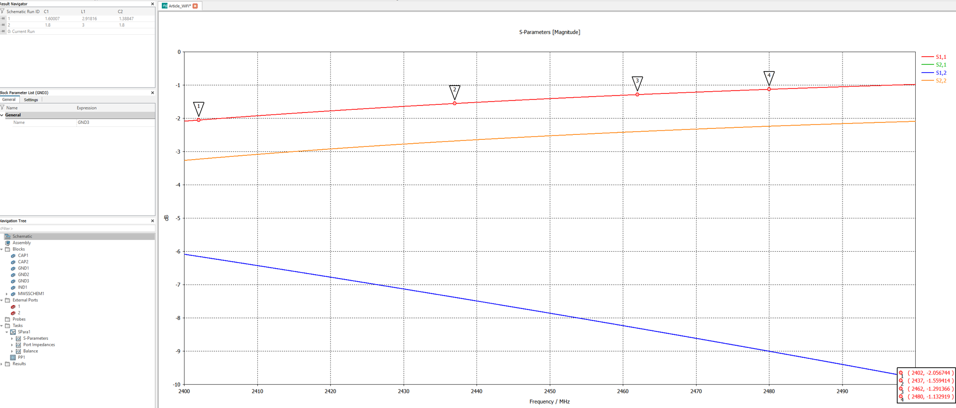
In CST Studio Suite, open the co-simulation setup and connect the ideal components to the corresponding connection points defined in the previous step. Configure the simulation to use the frequency domain solver over the same range established in Stage 1: 2400 MHz to 2500 MHz, with evaluation points at 2402, 2437, 2462, and 2480 MHz.
Run the simulation and open the S-Parameters result. Compare the S1,1 response against the Stage 1 baseline. The differences observed at this point are attributable entirely to the layout, the component values have not changed, so any frequency shift, impedance deviation, or degradation in the S1,1 response reflects the parasitic effects introduced by the physical PCB structure: trace inductance, pad capacitance, coupling between adjacent conductors, and discontinuities at bends and transitions.
This is the first simulation in the workflow that reveals what the board itself contributes to the filter response.
Re-Optimization Under Layout-Aware Conditions
The parasitic effects introduced by the layout will generally shift the filter response away from the optimized target established in Stage 1. The component values that produced the best S1,1 in the ideal schematic domain are no longer optimal when the physical environment is included in the simulation.
To recover the target response, repeat the optimization process using the same CST optimizer configured in Stage 1, CMA Evolution Strategy, with the four Wi-Fi 2.4 GHz channel centers as optimization targets and the Espressif-recommended value ranges as boundaries. This time, however, the optimizer operates on the co-simulation model: each evaluation includes the full electromagnetic contribution of the layout, so the resulting component values will implicitly compensate for the parasitic effects of the board.
Run the optimizer and allow it to converge. The new values of C1, C2, and L1 will differ from the Stage 1 results, in some cases significantly, and these differences are themselves informative: they quantify the degree to which the physical layout perturbs the filter behavior and the extent of the correction required to restore the target response.
Like in the first article, let’s optimize these component values, the optimizer can use the same configuration as before.
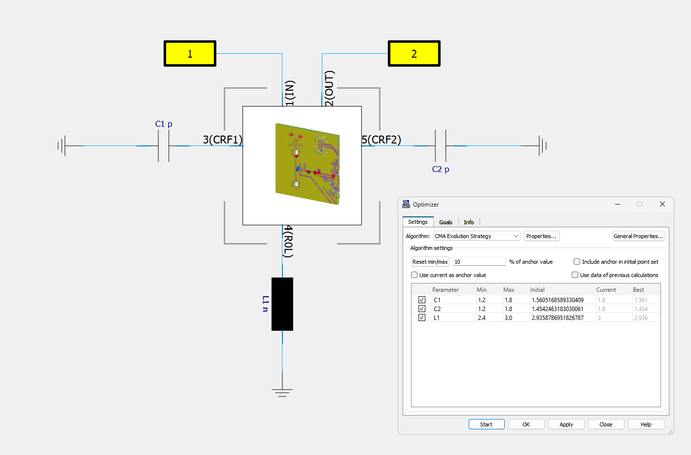
When the optimizer finishes, open S-Parameters and verify that the S1,1 target has been recovered across the four channel frequencies. Record the new component values for use in the Altium update that follows.
Update in Altium
With the layout-aware optimized values confirmed in CST, the next step is to propagate these results back into the Altium Designer project.
Open the ESP32-S3 schematic and update the component values of CRF1, CRF2, and the series element to reflect the new optimized results. If the re-optimization produced values that differ from the standard commercial series available from Murata or equivalent suppliers, select the nearest available standard value and note the deviation, this will be relevant in Stage 3, where real component models replace ideal ones.
After updating the schematic, synchronize the changes to the PCB file and review the component placement. If the re-optimization revealed sensitivity to parasitic coupling between specific components, this is the appropriate point to evaluate whether placement adjustments can reduce that coupling before Stage 3. Similarly, review the RF routing for any geometry that the co-simulation identified as a significant contributor to parasitic effects, trace length, bend geometry, and via placement are the most common sources.
Comparison with Stage 1
With both stages complete, a direct comparison between the Stage 1 and Stage 2 results can now be made. This comparison is the central deliverable of this article, it makes visible the gap between ideal schematic behavior and layout-aware co-simulation behavior, and quantifies what the physical PCB structure contributes to the filter response independently of component tolerances or material losses.
Plot the S1,1 magnitude curves from both stages on the same axis. Four indicators are worth examining in sequence. The first is frequency shift: the parasitic inductance of the RF routing and the parasitic capacitance of the component pads tend to shift the filter response downward in frequency relative to the ideal schematic prediction, the markers at 2402, 2437, 2462, and 2480 MHz make this shift immediately visible. The second is S1,1 magnitude variation at those four frequencies, which reflects how much the impedance match degrades when the physical environment is included. The third is bandwidth change, whether the parasitic effects have narrowed or broadened the matched region. The fourth is the Smith Chart trajectory, which reveals whether the impedance locus has rotated, compressed, or distorted relative to the Stage 1 result.
It is worth noting that the Stage 2 model includes the RF switch PE4259 connected via its Touchstone model, which means the comparison also captures the insertion effect of the switch on the signal path, an effect that was entirely absent from the Stage 1 schematic. This makes the Stage 2 result more representative of the actual signal chain, not only of the filter in isolation.
Together, these indicators establish a clear picture of what the layout and the surrounding circuit contribute to filter behavior, and why schematic-level optimization alone is insufficient for a design that will be manufactured and measured on a real board.
Closing
This second stage introduced the first layer of physical reality into the workflow. By importing the PCB layout from Altium into CST Studio Suite and running a co-simulation with ideal components, it became possible to isolate what the board geometry and the RF signal chain contribute to the filter response, independently of component tolerances or material losses, which are not yet part of the model.
Three things were established that did not exist after Stage 1. First, a simulation model that includes the actual copper geometry, dielectric stack, and pad shapes of the ESP32-S3 board. Second, the PE4259 RF switch connected in the signal path via its manufacturer Touchstone model, making the simulation representative of the real circuit topology rather than an isolated filter. Third, a re-optimized set of component values that account for the parasitic effects of the physical implementation, values that are more representative of what the real board will require than the Stage 1 results.
The differences between the Stage 1 and Stage 2 S1,1 responses are not a problem to be corrected: they are information. They quantify the contribution of the layout and the switch, and they define the starting point from which Stage 3 will work.
In Stage 3, the remaining layer of abstraction is removed. Ideal components are replaced by real manufacturer models downloaded from Murata's SimSurfing database, introducing finite Q-factors, self-resonance frequencies, and frequency-dependent losses into the simulation. A full 3D electromagnetic analysis, including E-field, H-field, surface current distribution, and power loss density, will complete the model and establish the foundation for the EMI analysis that follows.
That is where the design stops being a co-simulation and starts becoming a map of the electromagnetic structure of the real board.
Getting from an ideal filter to one that survives fabrication is the work our Advanced R&D Labs does for hardware teams. If your board came back measuring differently than it simulated, tell us what you're seeing.