RF Filter Design for ESP32-S3, Part 1: The Ideal Filter and First Layout
An ESP32-S3 RF filter that passes simulation can still fail on the fabricated board. Part 1 of this series builds the foundation: a CLC PI filter designed in CST Studio Suite, optimized with CMA-ES across the 2.4 GHz Wi-Fi channels, and carried into a controlled-impedance Altium layout.

This is Part 1 of a three-part series on ESP32-S3 RF filter design. Part 2 covers PCB effects and EM co-simulation.
Topology definition and electrical baseline without physical effects
"It requires a much higher degree of imagination to understand the electromagnetic field than to understand invisible angels. I speak of the E and B fields and wave my arms and you may imagine that I can see them, but I cannot really make a picture that is even nearly like the true waves."
— Richard Feynman, The Feynman Lectures on Physics, Vol. II (1964)
Problem
In early 2024, a hardware team reached out to Altiv Labs after their ESP32-S3 IoT product came back from fabrication with a filter response significantly worse than simulated. The matching degraded progressively from 2402 MHz toward 2480 MHz, a classic symptom of layout parasitics shifting the response. Two bench component swaps had produced partial improvement, but no systematic understanding of why. The question they brought was direct: how do we know, before the next board revision, what values will actually work?
Answering it required a model that included the electromagnetic behavior of the PCB layout, the real insertion effect of the RF switch, and the frequency-dependent behavior of the specific commercial components to be soldered, not ideal elements, not approximations.
Designing an RF filter for a Wi-Fi 2.4 GHz system looks straightforward on a schematic. The CLC PI topology is well understood, the target frequencies are fixed, and component values can be calculated analytically. The problem is that what meets the S1,1 target on screen rarely meets it on a board.
That model exists in CST Studio Suite. But the complete workflow to build it, ODB++ import from Altium, 3D model trimming, discrete port placement, EM co-simulation with the schematic environment, re-optimization against real Wi-Fi channel targets, and final conversion of ports to SPICE-based Lumped Elements using manufacturer models from Murata SimSurfing, is not documented in any consolidated, publicly available source. Fragments exist in official documentation and forum threads, but the operative connections between steps are absent.
This series closes that gap. It provides a reproducible, end-to-end methodology for RF engineers and researchers who need simulation predictions grounded in the same physics a VNA observes, before the board is built.
Introduction
Modern embedded RF systems typically operate across multiple signal paths simultaneously. A representative platform such as the ESP32, for instance, integrates Bluetooth, Wi-Fi, and often coexists with external RF front-end components, including switches and matching networks, all within a single compact design.
At the schematic level, designing an RF filter or matching network may initially appear straightforward. Component values can be calculated analytically, transfer functions look clean, and performance targets seem well within reach. However, this result exists purely in a mathematical domain, one that makes no concessions to physical reality.
Once the design is transferred to an actual PCB, a range of non-ideal effects begin to govern circuit behavior. Transmission lines introduce distributed phenomena, passive components exhibit parasitics and finite Q-factors, and the physical layout itself becomes an active part of the electromagnetic system, whether the designer accounts for it or not.
This is precisely where electromagnetic simulation becomes indispensable. Tools such as CST Studio Suite allow engineers to move beyond ideal assumptions and incrementally incorporate physical constraints into the design flow. By merging circuit-level simulation with full-wave electromagnetic analysis, they enable a controlled, progressive transition from schematic to manufacturable PCB.
This article presents a structured methodology for RF filter development, beginning with an ideal circuit topology, advancing through layout-aware simulation stages, and culminating in a model that accurately reflects real hardware behavior. At each step, additional physical effects and constraints are introduced, allowing the designer to understand not only how the circuit performs, but why it behaves the way it does.
RF architecture definition
The starting point for this workflow is the RF architecture recommended by Espressif for the ESP32-S3, taken directly from the hardware design guidelines. According to that reference, the RF circuit is composed of three main parts: the RF trace on the PCB, the chip matching circuit, and the antenna with its associated matching network. Espressif specifies that the RF trace should be controlled to 50 Ω, that the chip matching circuit must be placed close to the chip, and that a CLC structure is preferred for the chip-side network, used to adjust the impedance point and suppress harmonics.
Adopting this topology as the baseline rather than an arbitrary lumped network gives the design a stronger engineering foundation. The first schematic is not an academic exercise, but a structure derived directly from the intended RF integration method of the device.
At this stage, the scope is deliberately limited to the chip-side matching and filter behavior. Variables such as RF switching, broader front-end interactions, and complex routing constraints are intentionally excluded, not because they are irrelevant, but because isolating the filter first makes the evolution from ideal circuit to physical implementation traceable and attributable. It is also worth noting that Espressif ties the final component values explicitly to the actual antenna and PCB layout, which means the topology defined here should be treated as a starting structure, not a fixed solution. That is precisely what the CST optimization workflow addresses in the following sections.
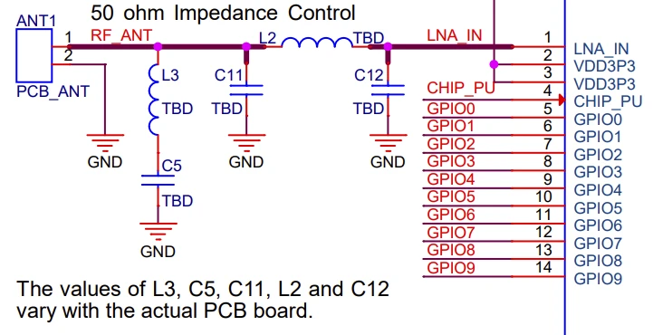
Schematic construction in CST Studio Suite
With the RF topology defined, the next step is to translate it into the CST Studio Suite schematic environment. The objective at this stage is to build a clean, simulation-ready circuit model using the ESP32-S3 RF structure as the electrical reference, before any physical effects are introduced.
CST Project Template Definition
Before opening the schematic editor, the project must be configured with the correct template. This establishes the simulation environment and ensures that the frequency range, units, and solver settings are aligned with the 2.4 GHz Wi-Fi and Bluetooth bands targeted by the ESP32-S3.
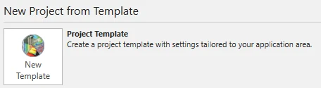
Start a new project with New Template.
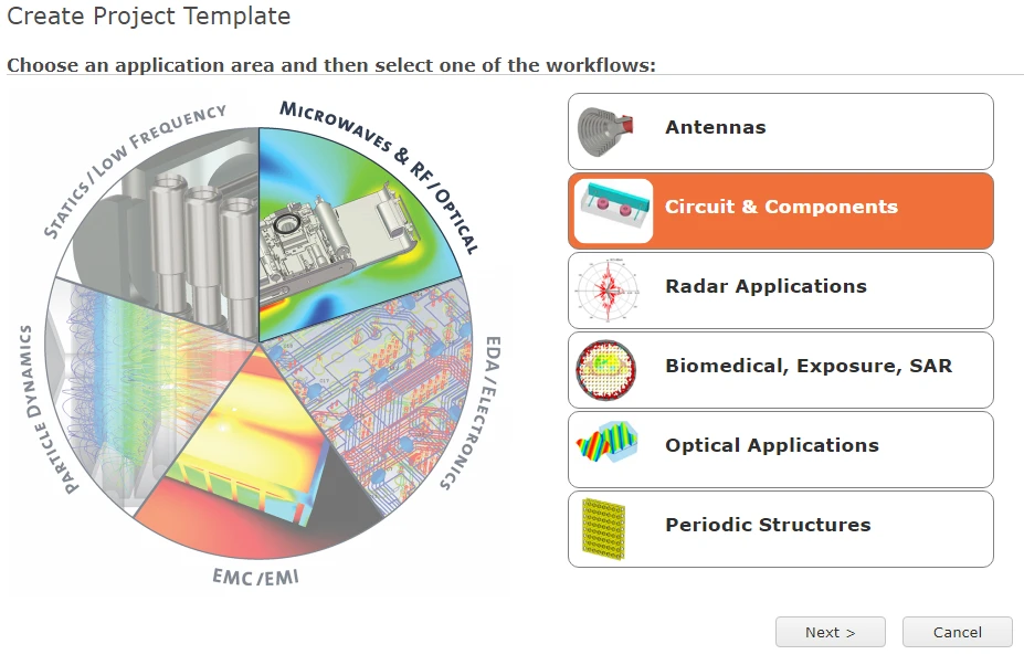
In the template wizard, select:
Microwaves & RF/Optical → Circuit & Components
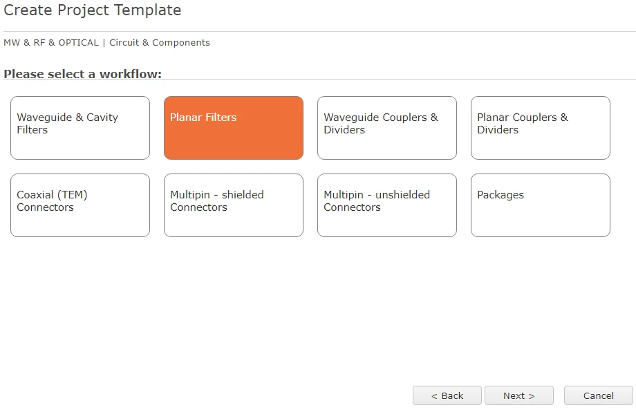
For the workflow, select:
Planar Filters
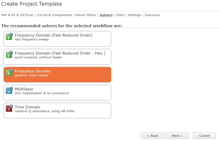
In the solver step, select:
Frequency Domain
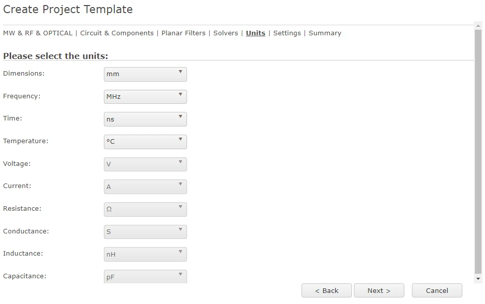
In the units step, use:
- Dimensions: mm
- Frequency: MHz
- Time: ns
- Temperature: °C
- Voltage: V
- Current: A
- Resistance: Ω
- Conductance: S
- Inductance: nH
- Capacitance: pF
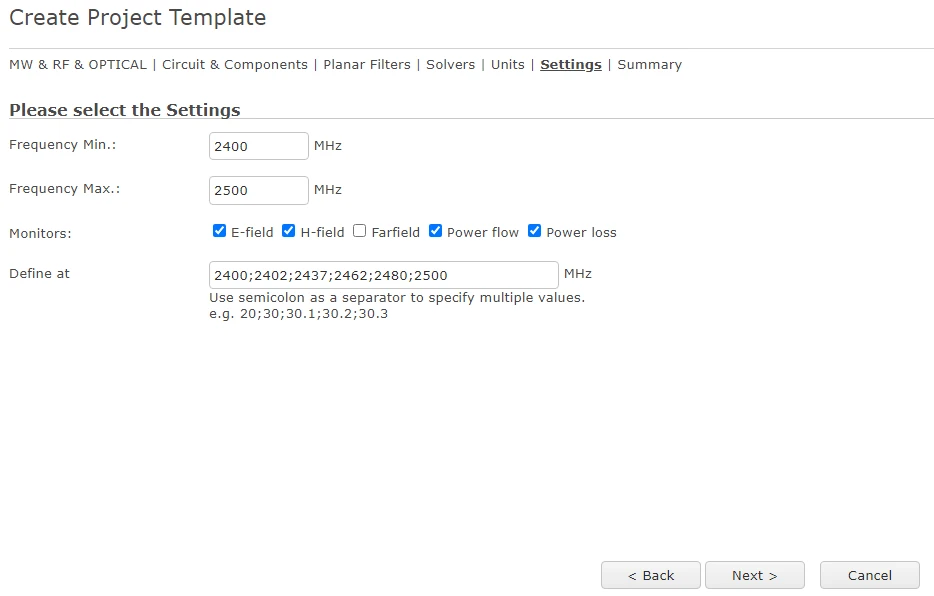
In the settings step, define:
- Frequency Min: 2400 MHz
- Frequency Max: 2500 MHz
Enable these monitors:
- E-field
- H-field
- Power flow
- Power loss
Leave Farfield disabled.
In Define at, enter:
2400;2402;2437;2462;2480;2500
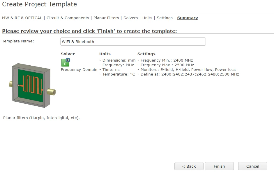
These six values correspond to the band edges and the four main Wi-Fi 2.4 GHz channel centers, the same frequencies that will later be used as optimization targets. Once the summary is confirmed, click Finish to complete the template setup.
Filter construction with ideal components (L and C)
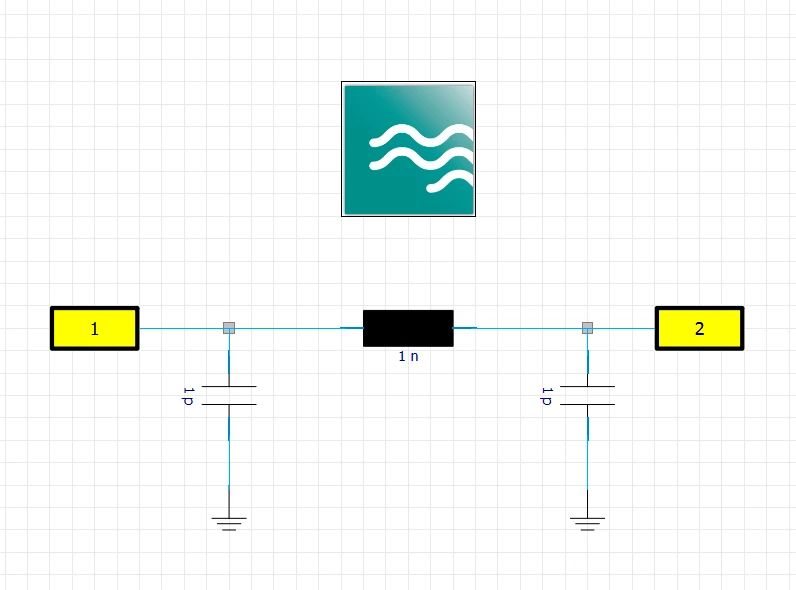
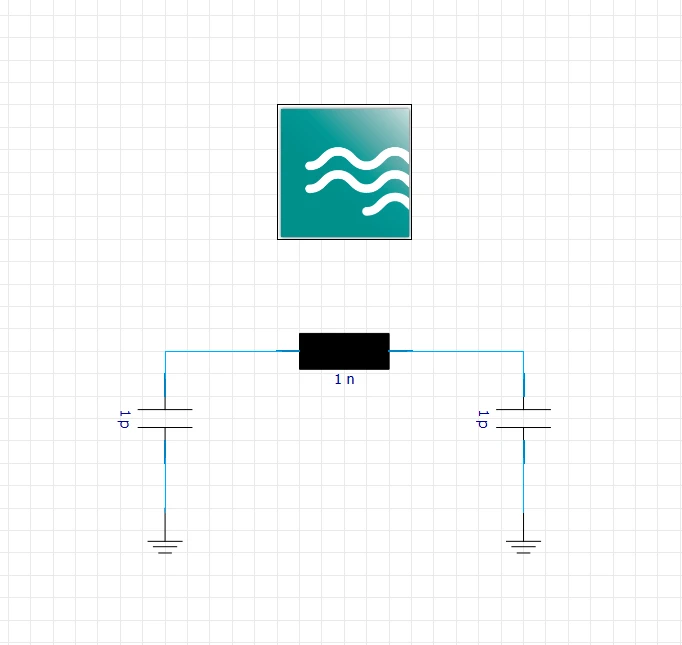
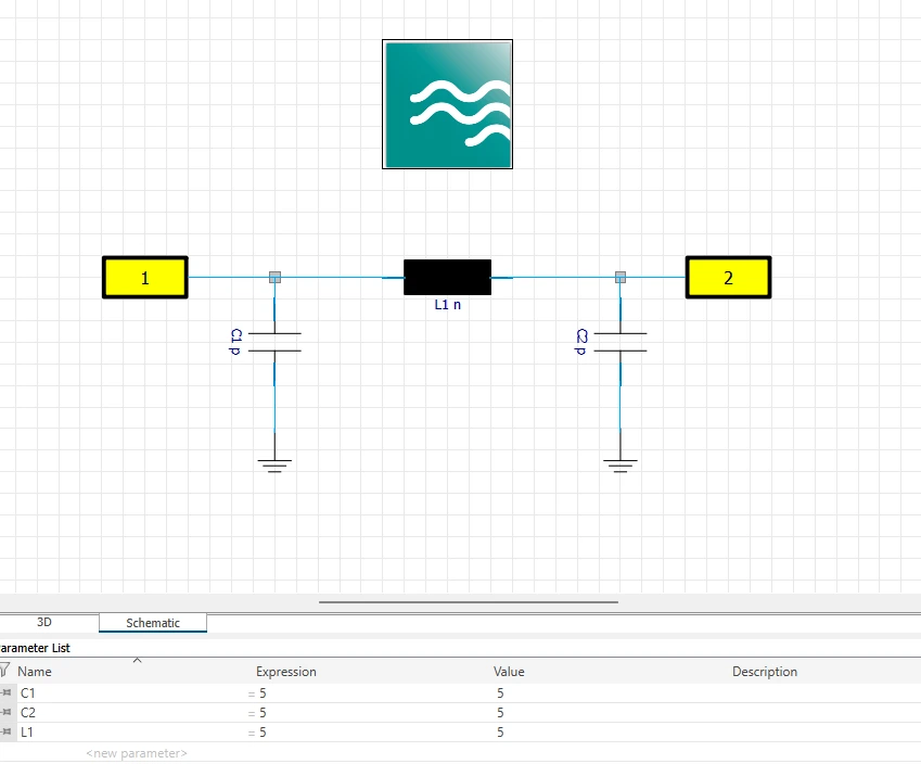
With the project template configured, the next step is to build the filter in the CST schematic environment using ideal lumped components. The objective is to implement the CLC network in a PI configuration, two shunt capacitors to ground flanking a series inductor, which is the chip-side topology recommended by Espressif for the ESP32-S3.
Open the Schematic tab at the bottom of the screen to switch into the circuit construction view.
In the left-side panel, open the Block Selection Tree and expand Circuit Elements, as shown below. This is the component library used for ideal lumped elements.
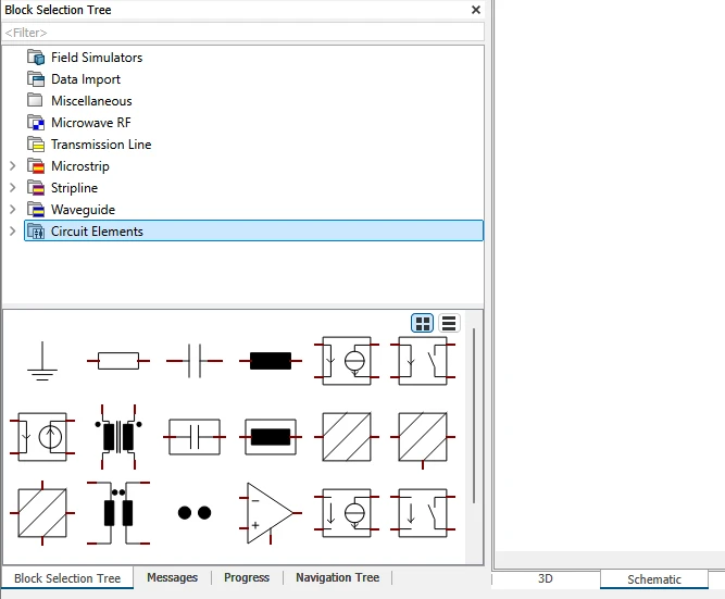
From this library, place two capacitors and one inductor to form the PI network.
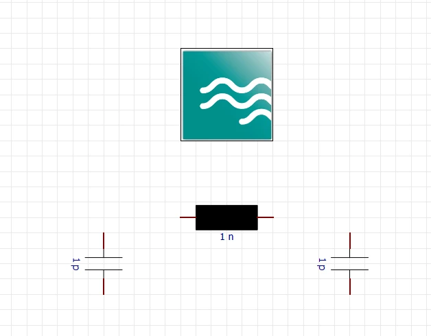
Connect the components to define the signal path, then press G to place ground symbols on the shunt capacitor nodes.
Finally, press P to place Port 1 at the chip-side input and Port 2 at the filter output. These ports define the excitation and termination points required for the S-parameter simulation.
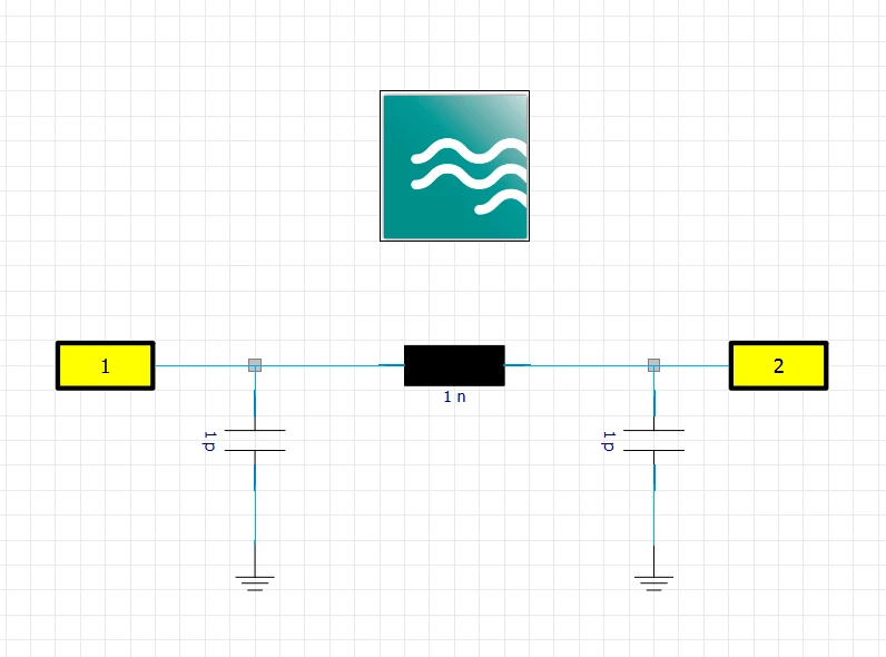
At the end of this step, the first ideal version of the filter is ready in the CST schematic environment.
Initial simulation
With the CLC filter assembled in the schematic, the next step is to parameterize the components and run the first S-parameter simulation. This generates the initial reference response, the baseline against which all subsequent optimizations will be compared.
Start by opening the property dialog of each component and replacing the fixed value with a parameter name. This makes the circuit easier to modify and prepares it for the optimization step that follows.
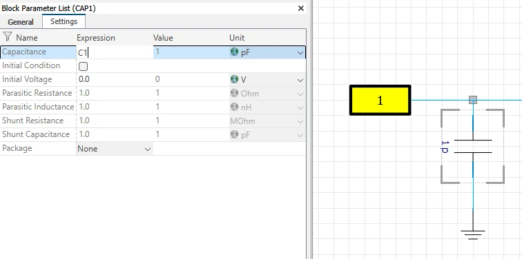
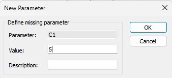
After naming all parameters, a prompt will appear asking for an initial value for each one. Use 5 as the starting point for all three, this is a placeholder that simply needs to be within a plausible order of magnitude, since the optimizer will determine the final values in the next stage.
Confirm that all three parameters appear correctly in the Parameter List at the bottom of the screen before proceeding.
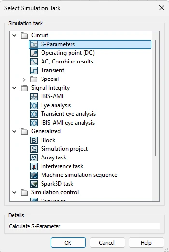
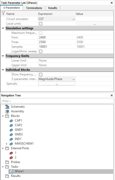
To run the simulation, create a new task. In the Select Simulation Task dialog, choose S-Parameters under the Circuit category.
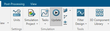
Define the task settings using the project frequency range, then click Update to run the first simulation.
When the simulation completes, open the S-Parameters result and select the Smith Chart view to observe the initial impedance behavior of the circuit.
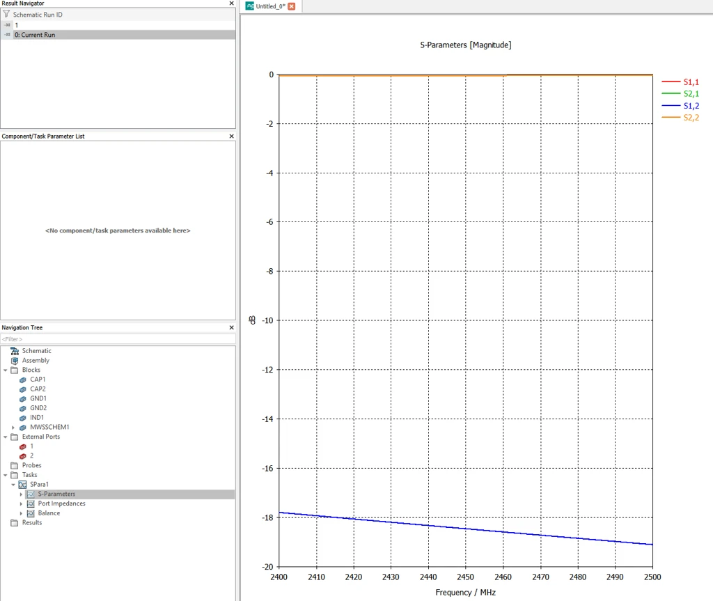
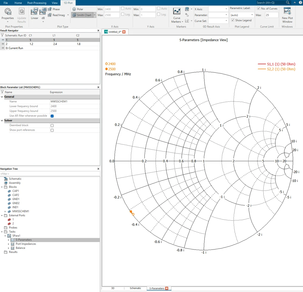
At this point the first simulation baseline is established. This response reflects the behavior of the filter at arbitrary starting values and will serve as the reference for the adjustments that follow.
Initial optimization
With the baseline response established, the next step is to refine the component values within the ranges recommended by Espressif and run the first optimization focused on improving S11 across the 2.4 GHz Wi-Fi channel frequencies.
Adjustment of L and C for best S11
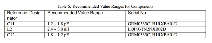
Start by replacing the placeholder values with the limits from Table 6 — Recommended Value Ranges for Components, from the ESP32-S3 hardware design guidelines. These ranges define the minimum and maximum boundaries that the optimizer will respect.
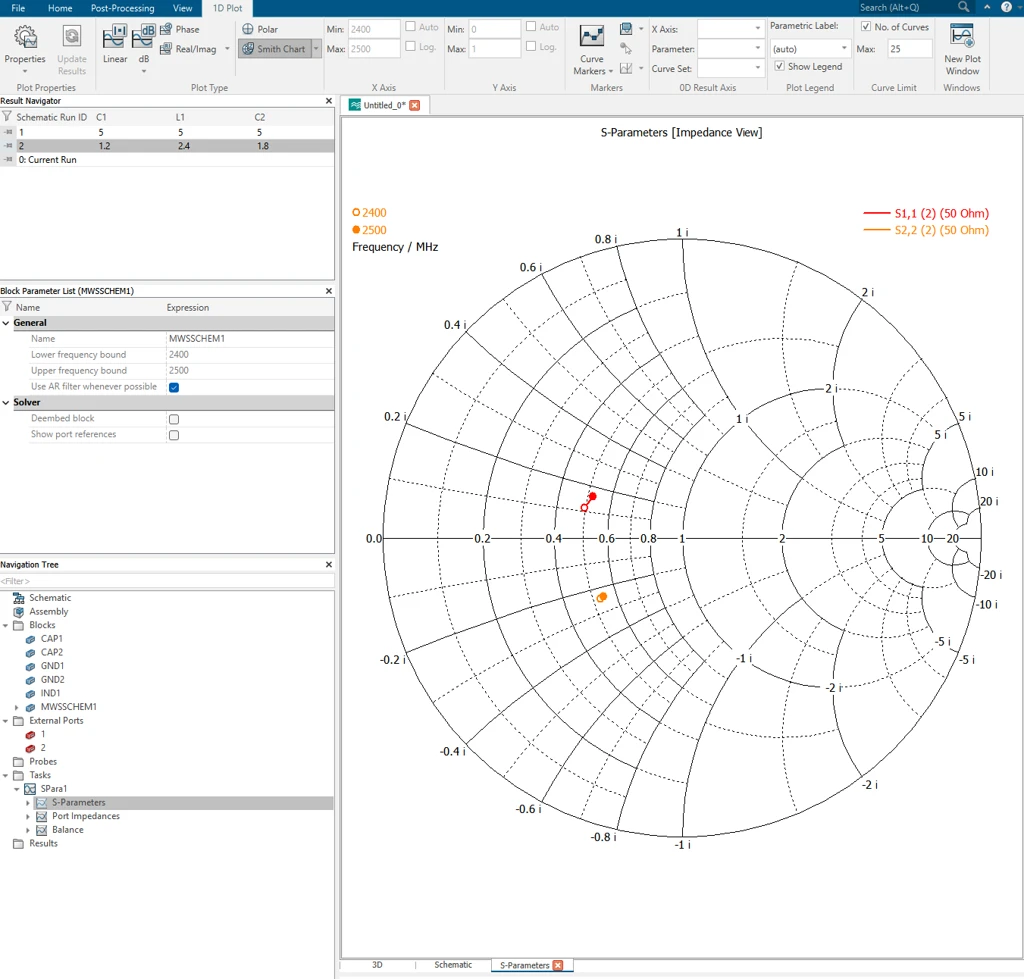
Click Update and open the S-Parameters result to compare the new response with the previous baseline.
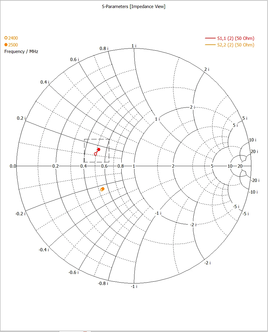
Zoom in around the S1,1 curve to inspect its behavior more clearly.
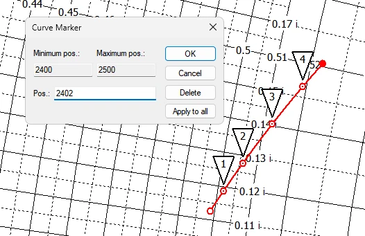
To define the optimization targets, open Curve Markers and place four points on the S1,1 curve one at each of the main Wi-Fi 2.4 GHz channel centers: 2402, 2437, 2462, and 2480 MHz. These are the frequencies at which the optimizer will evaluate and minimize the reflection coefficient.
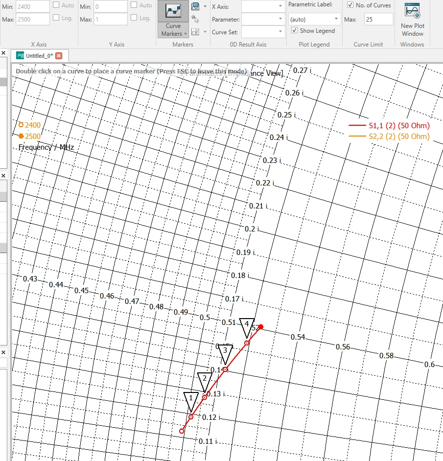
Press Esc, then double-click each marker to open its property dialog and confirm the target frequency.
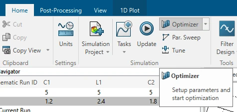
To open the optimizer, go to the Home tab and click Optimizer.
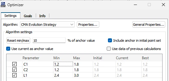
In the Settings tab, select CMA Evolution Strategy as the algorithm. Then enable the three circuit parameters and set their minimum and maximum limits using the Espressif ranges from Table 6.
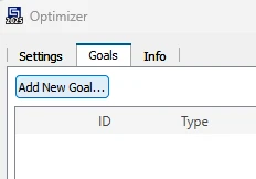
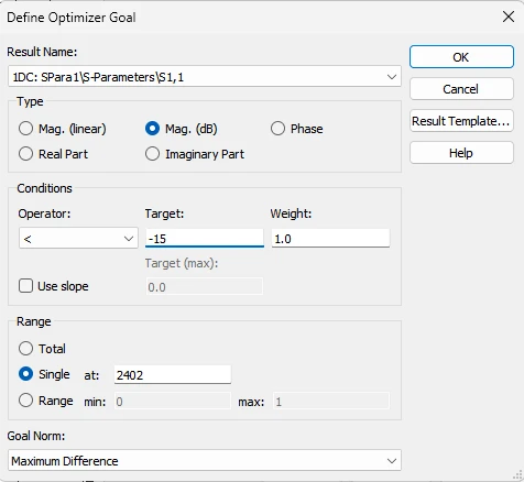
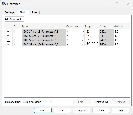
Go to the Goals tab and click Add New Goal. For each of the four target frequencies, create a goal with the following configuration: Type Mag. (dB), Operator <, Target −15, Range Single at the corresponding frequency.
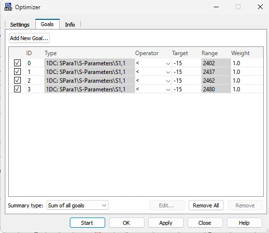
Click Start to begin the optimization. CST will evaluate combinations of C1, C2, and L1 within the defined ranges until the S1,1 target is met at all four frequencies.
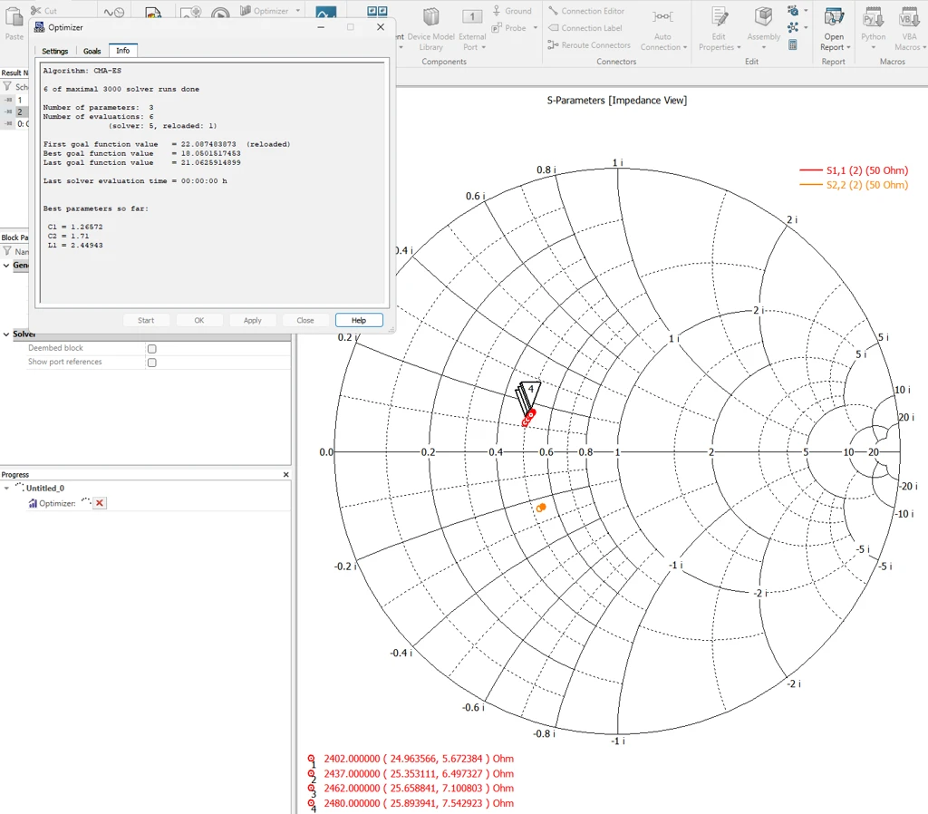
When the optimizer finishes, open S-Parameters again to inspect the updated result.
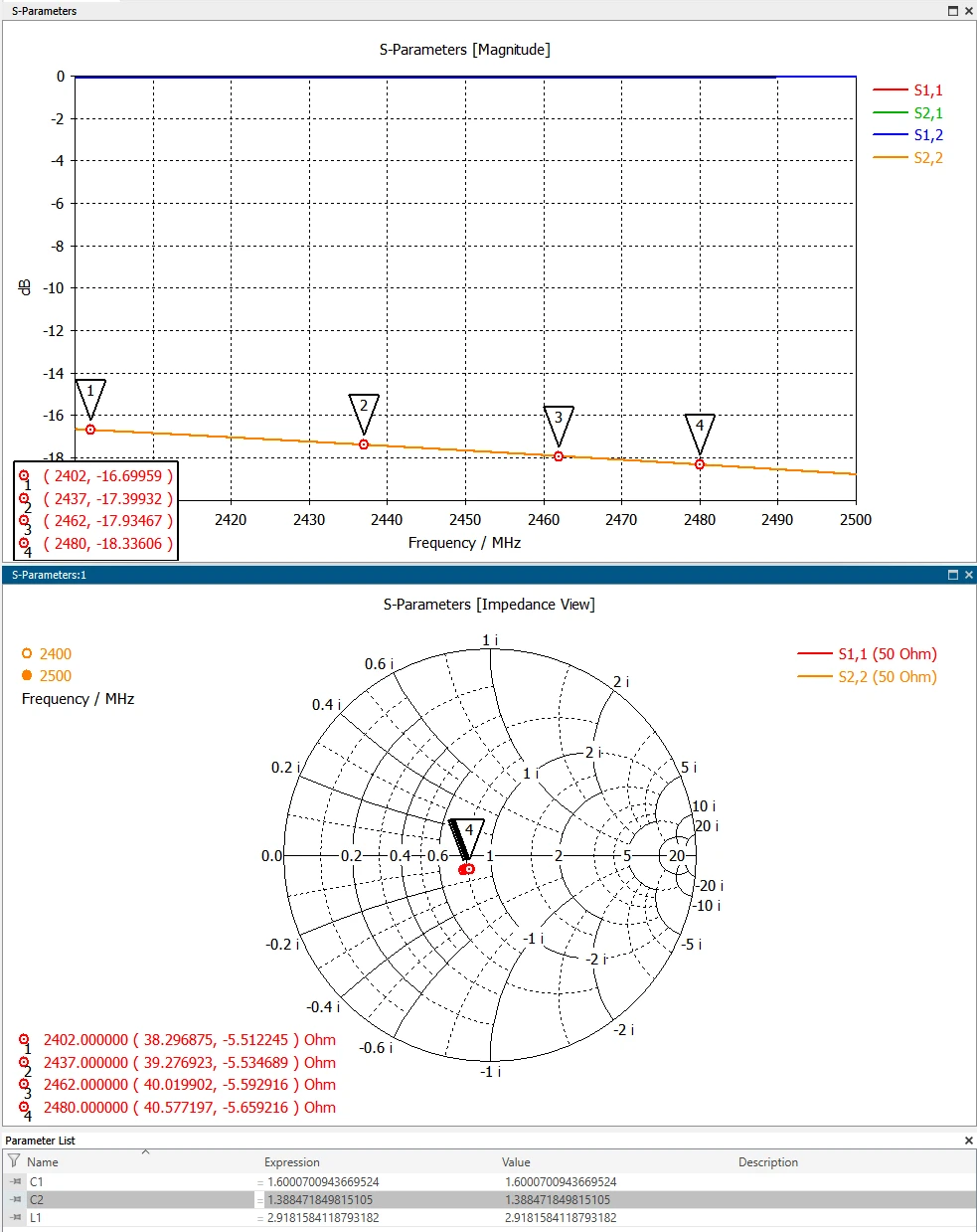
If a stronger matching target is needed, the same process can be repeated by changing the Target value in the optimization goals to more aggressive levels such as −20 dB, −25 dB, or −35 dB and running the optimizer again. The example below shows the result obtained with a −25 dB target, where the optimizer converged to C1 = 1.8 pF, C2 = 1.8 pF, and L1 = 3 nH.
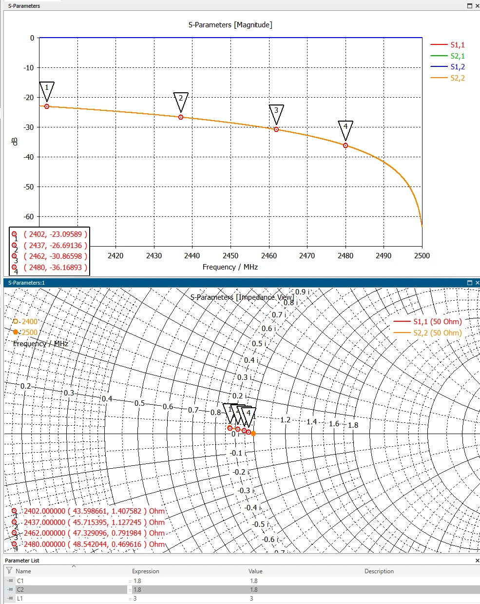
At this point the first optimized version of the ideal filter is complete. The component values obtained here will serve as the electrical reference for the PCB implementation in the following stage.
Implementation in Altium
With the optimized filter topology defined in CST Studio Suite, the next step is to transfer this circuit into Altium Designer and create the first PCB implementation. This stage marks the transition from a purely circuit-based model to a physical design environment, where component placement, RF routing, and board stackup begin to influence the feasibility of the solution.
Schematic creation using optimized values
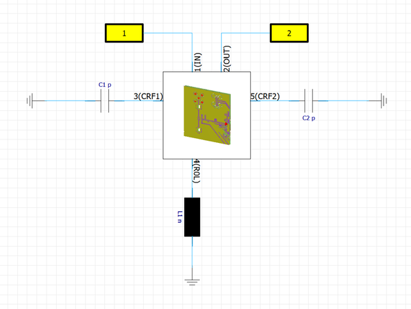
Inside the ESP32-S3 project schematic in Altium Designer, create the filter circuit using the topology optimized in CST. The PI structure is implemented as follows: a shunt capacitor to ground at the input (CRF1), a series element in the line (R0L), and a shunt capacitor to ground at the output (CRF2).
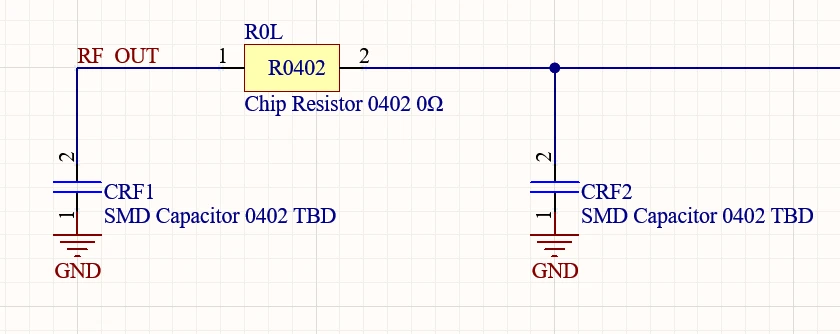
The series element is represented by a 0 Ω resistor footprint in the R0402 package. This placeholder preserves the correct pad geometry and routing footprint for the series position, while allowing the component to be replaced by an inductor during layout refinement or laboratory adjustment without requiring a PCB respun. At this stage, the inductor value is known from the CST optimization, but its final placement and routing will be validated in the next article when the layout is imported back into CST.
At this point the objective is only to reproduce the optimized electrical structure inside the ESP32-S3 hardware project, keeping the same topology already validated in the CST schematic.
Impedance Definition
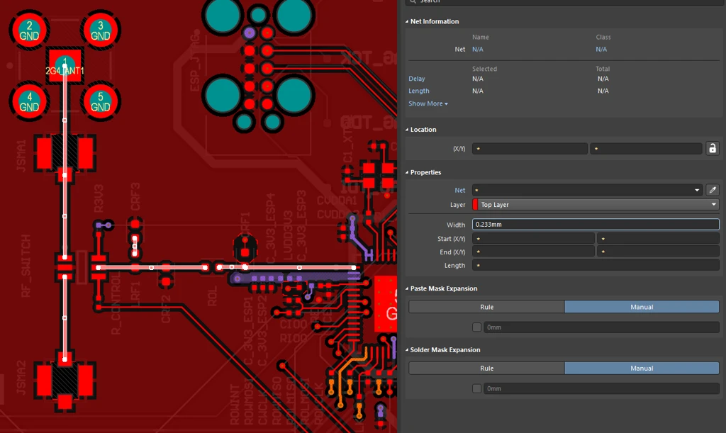
After creating the filter schematic, define the PCB impedance rule that will control the RF trace geometry. The objective is to establish a 50 Ω transmission line in the ESP32-S3 PCB layout, consistent with the controlled impedance requirement specified by Espressif for the RF trace.
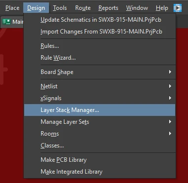
In the PCB file, go to Design → Layer Stack Manager.
Inside the Layer Stack Manager, open the Impedance tab at the bottom of the window.
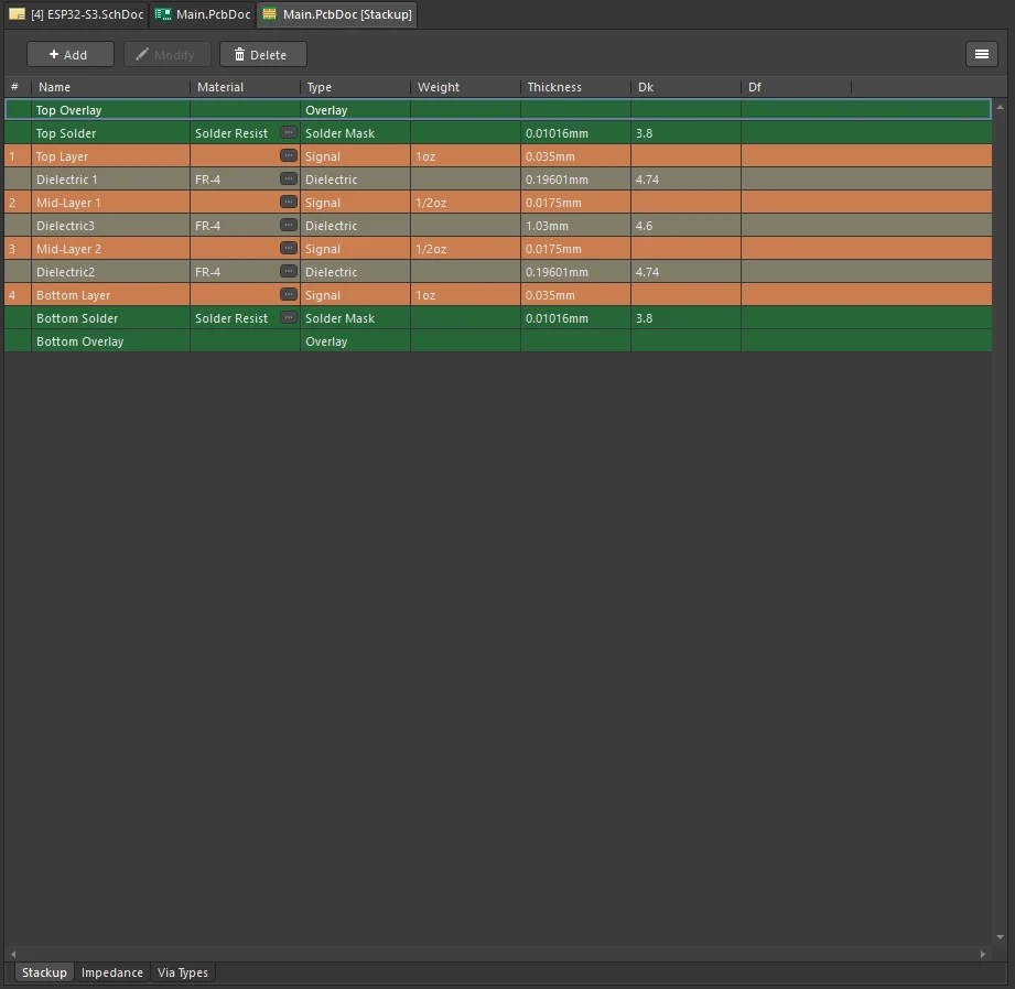
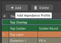
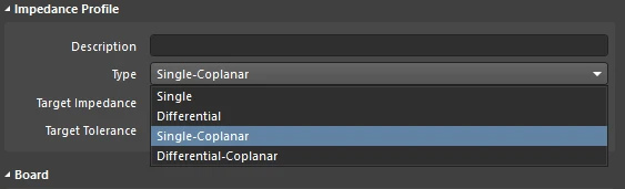
Click Add Impedance Profile. In the profile settings, select Type: Single-Coplanar and set the Target Impedance to 50 Ω.
Altium calculates the trace geometry required to reach the target impedance based on the board stackup and displays the corresponding Width value for each layer combination.
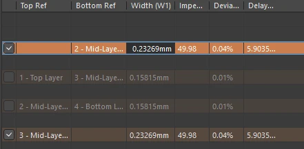
Use the width value from the layer that will carry the RF traces as the reference when routing the filter connections in the ESP32-S3 layout.
Closing the First Article
This first stage of the workflow established the electrical foundation for the RF filter design. Starting from the chip-side topology recommended by Espressif for the ESP32-S3, it was possible to build an ideal CLC filter in CST Studio Suite, simulate its initial response, optimize the lumped component values for improved S11 behavior across the four main Wi-Fi 2.4 GHz channels, and transfer the result into Altium Designer as the first physical implementation of the circuit. With the RF trace impedance defined at 50 Ω, the layout already reflects a more controlled starting point than an unoptimized implementation would provide.
The value of this stage lies not in reaching final hardware performance, but in establishing a coherent and traceable path from the reference topology to a manufacturable PCB. Each decision made here the choice of topology, the optimizer targets, the impedance definition has a documented rationale that will make the next stages easier to interpret and validate.
Part 2 picks up there: importing the layout into CST for EM co-simulation, the PCB created in Altium will be exported and imported into CST Studio Suite, where the physical layout will begin to participate directly in the electromagnetic simulation. Routing geometry, pad shapes, copper transitions, and interconnect effects will become part of the model moving the analysis beyond the ideal schematic domain. The RF switch will also be introduced into the signal path at this stage, making the model more representative of the actual board.
That is where the design stops being an optimized circuit and starts becoming an RF structure shaped by the PCB itself.
If you're fighting a filter response that changed between simulation and fabrication, that's the kind of problem our Advanced R&D Labs takes on.