RF Filter Design for ESP32-S3, Part 3: Real Components and EMI Analysis
Ideal components cannot predict the losses and resonances of a fabricated RF filter. Part 3 evaluates frequency-dependent Murata 0402 models, selects practical component values, and transfers them into the CST 3D EM model to analyze S₁₁, EM fields, and power loss as a basis for EMI optimization.


Convergence toward real behavior and preparation for advanced EM analysis
"The practice of eliminating the physics by reducing a problem to a purely mathematical exercise should be avoided as much as possible. The physics should be carried on right through, to give life and reality to the problem."
— Oliver Heaviside, Electromagnetic Theory, Vol. 2 (1892)
Introduction
The first two stages of this workflow built a progressively more accurate model of the filter. Stage 1 established the ideal electrical baseline, a CLC network optimized in the schematic domain with no knowledge of the physical board. Stage 2 introduced the PCB layout into the simulation, revealing what the routing geometry, pad shapes, and copper transitions contribute to the filter response, and re-optimized the component values to account for those effects.
Both stages, however, shared one fundamental limitation: the components were ideal. They had no Q-factor degradation, no self-resonance, no frequency-dependent losses. The capacitors and inductor in the model behaved exactly as their nominal values describe, something that no physical component ever does.
This third stage removes that limitation. The ideal lumped elements are replaced by real manufacturer models sourced from Murata's SimSurfing database, introducing the finite Q-factors, parasitic series resistance, and self-resonance behavior that characterize actual SMD components in the 0402 package. With these models in place, the simulation for the first time reflects not only the electromagnetic environment of the board but also the electrical behavior of the components that will be soldered onto it.
The stage closes with a full 3D electromagnetic simulation, E-field, H-field, surface current distribution, and power loss density, and a three-way comparison across all stages that makes the progressive degradation from ideal to real fully visible.
Real Component Selection from Murata SimSurfing
The starting point for component selection is the set of optimized values obtained at the end of Stage 2. These values define the target around which the search in SimSurfing is conducted.
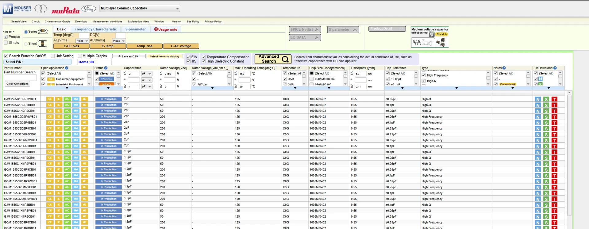
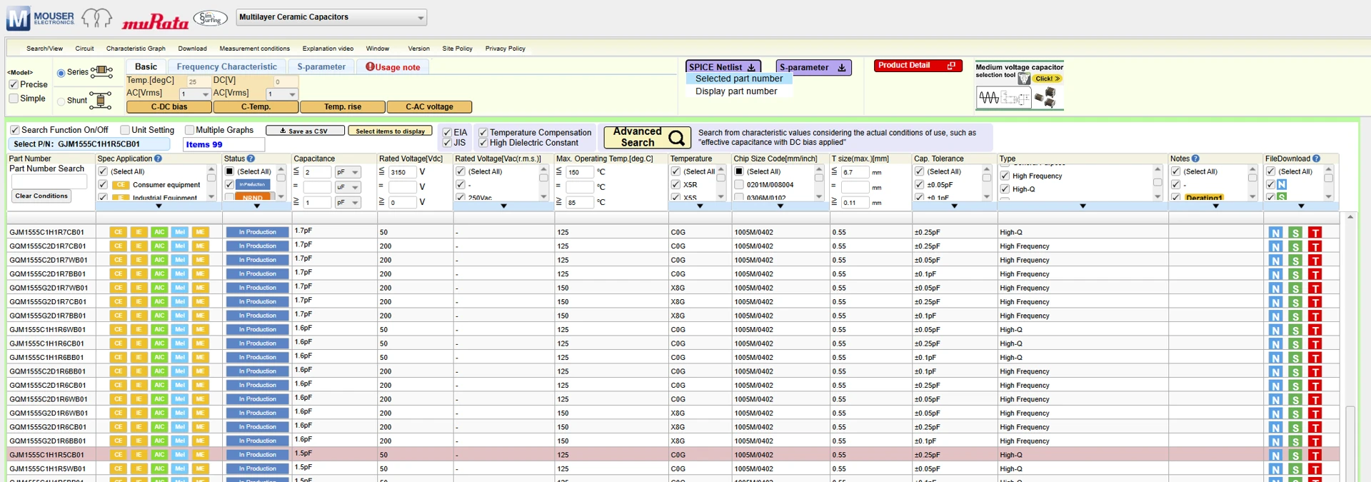
Access Murata SimSurfing at SimSurfing - Cap for capacitors and SimSurfing - Ind for inductors, and select the appropriate component category, capacitor for CRF1 and CRF2, inductor for R0L. In the search filters, apply the following constraints: Status: In Production, Chip Size Code: 1005M / 0402, Tolerance: < 5% / 0.5 pF / 0.5 nH, Type: High Frequency & High-Q. These filters ensure that the selected components are currently available, match the footprint already defined in the Altium layout, and have tolerances compatible with the precision required by the filter response.
Iterative Component Definition in CST
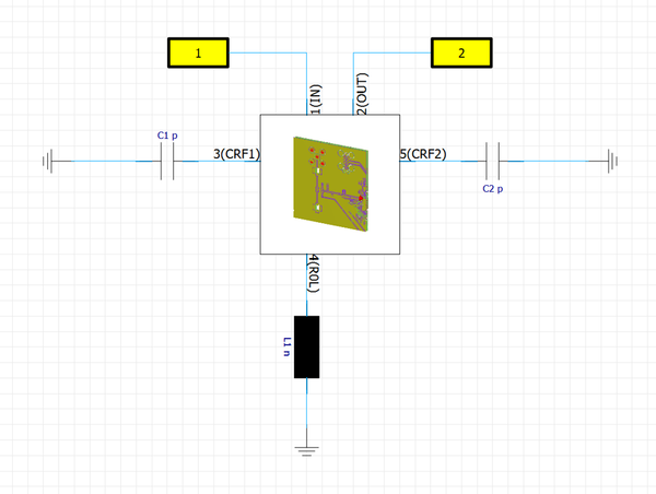
With the Stage 2 co-simulation complete and the optimized component values known, the next step is to find real manufacturer models that match those values and evaluate their effect on the S1,1 response. This process is done entirely in the Schematic environment first, not in the 3D model, because schematic-level updates are fast to modify and simulate, allowing rapid iteration across multiple component candidates before committing to the heavier 3D simulation.
The selection order follows the signal path: CRF1 first, then R0L, then CRF2.
Reading the current component value
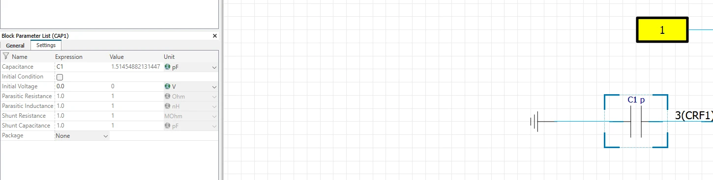
Open the Schematic tab and double-click CRF1 to open its Block Parameter List. In the Settings tab, note the current capacitance value, this is the optimized value obtained from Stage 2 and defines the center of the search range in SimSurfing.
Searching for a real component in SimSurfing
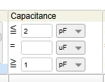
Access Murata SimSurfing and select the appropriate component category, capacitor for CRF1 and CRF2, inductor for R0L. Set the capacitance range to bracket the target value, for example, if the optimizer returned 1.5 pF, search between 1 pF and 2 pF. Apply the following filters: Status: In Production, Chip Size Code: 0402, Tolerance: < 5% / 0.5 pF / 0.5 nH.
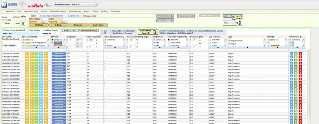
From the results list, select the component with the nominal value closest to the optimization target. For RF filter applications in the 2.4 GHz band, prefer C0G dielectric and High-Q type when available, as these characteristics indicate lower loss and more predictable behavior at high frequencies. Click SPICE Netlist and then Selected part number to download the model file.
Saving the model file
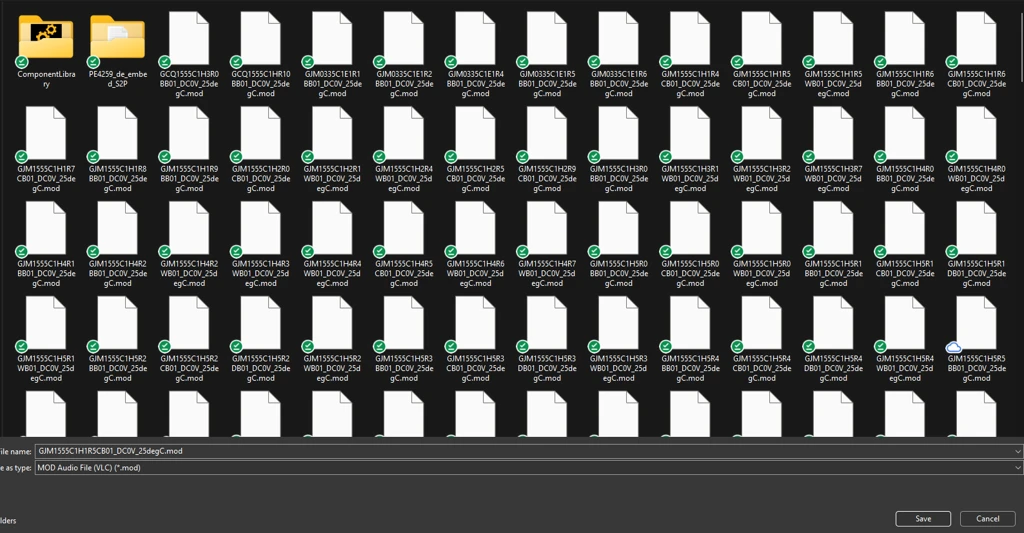
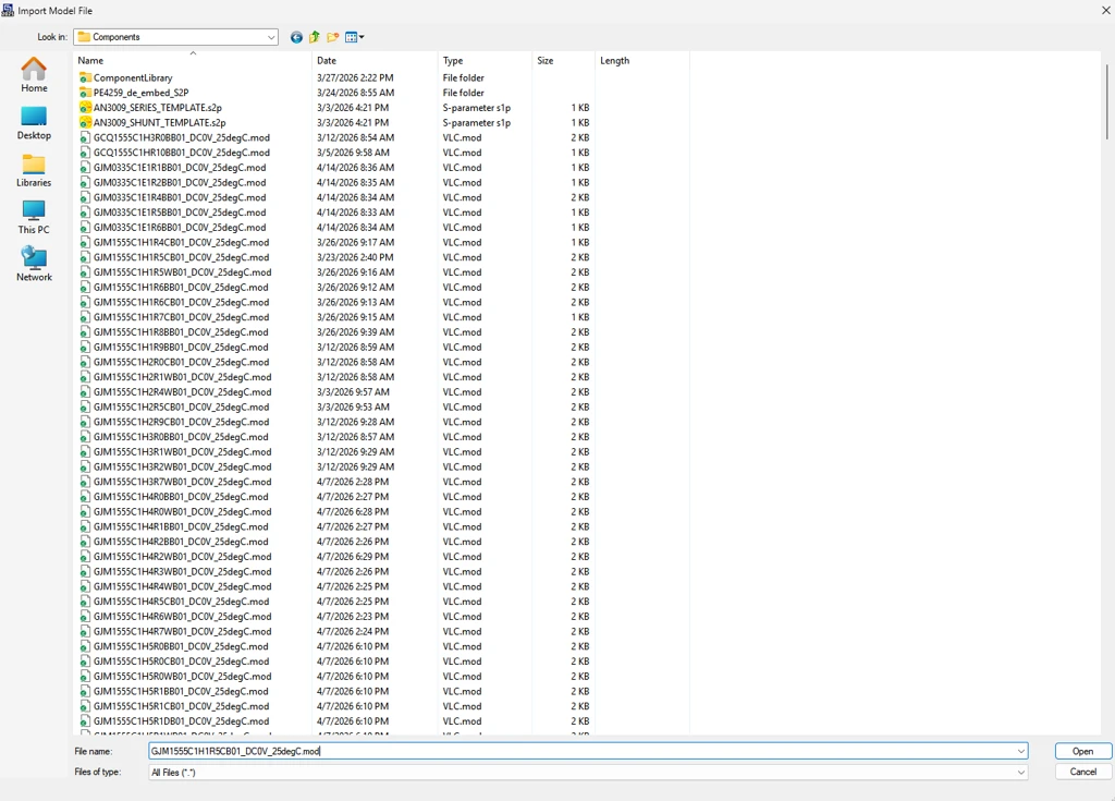
Before saving the downloaded file, copy the filename from the save dialog. When a component library grows to dozens of models accumulated across multiple projects, pasting the exact filename into the CST file browser is the fastest way to locate the correct model. Save the file to the folder where all component models are stored.
Importing the model into CST
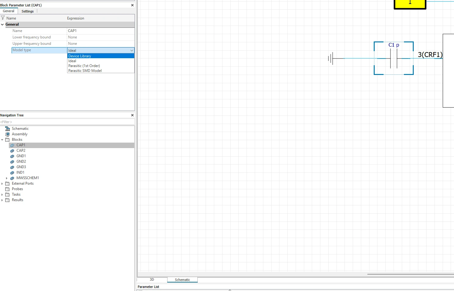
Back in CST Studio Suite, double-click CRF1 to open its Block Parameter List. Go to the General tab and change the Model type from Ideal to Device Library.
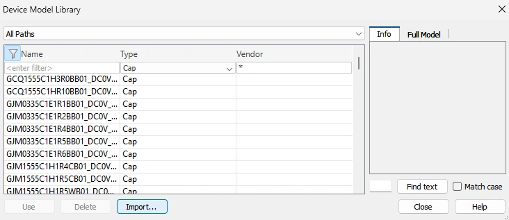
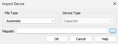
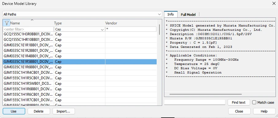
A Device Model Library window will appear. If the model has not been imported before, the list will not contain it yet, click Import.
In the Import Device dialog, click the three dots button next to Filepath.
Navigate to the components folder, paste the filename copied earlier into the File name field, and click Open.
With the model now visible and selected in the library, click Use to apply it to the component.
Evaluating the response
To evaluate the result, open the S-Parameters result and create a new Plot Window.
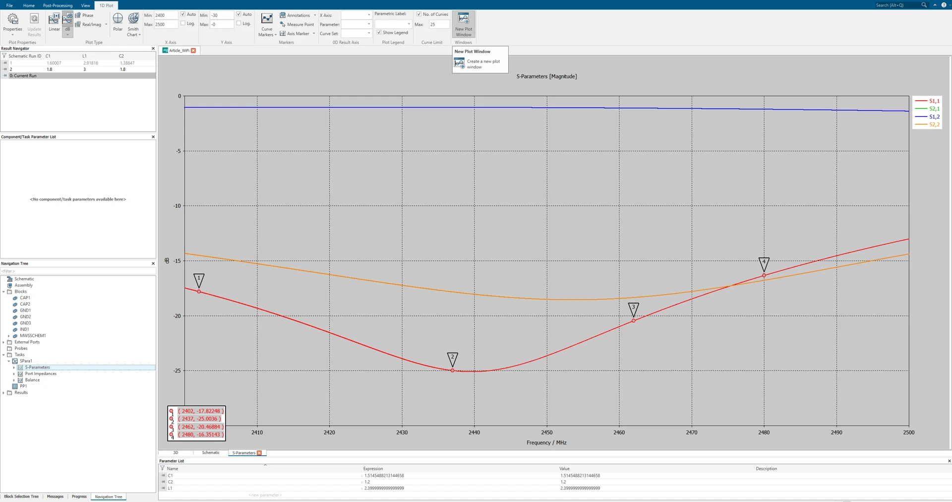
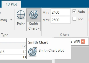
Select Smith Chart view in this new window.
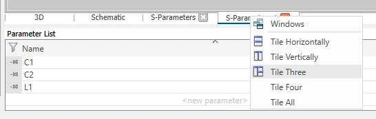
Then right-click the tab bar at the bottom and select Tile Three to display the schematic and both plot windows simultaneously.
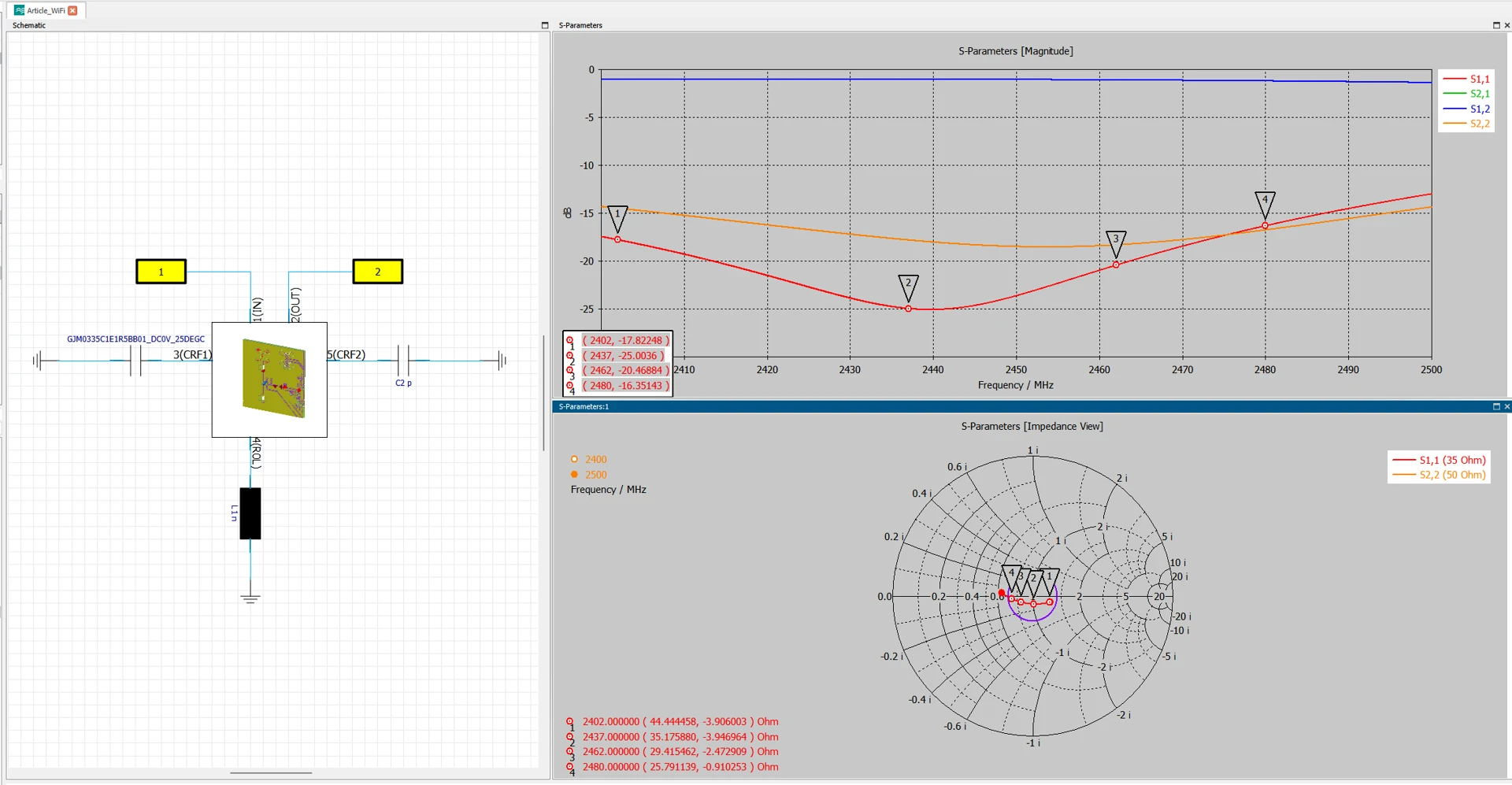
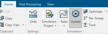
Click Update to run the simulation.
Monitor both the S1,1 magnitude curve and the Smith Chart. The component name from SimSurfing is now visible directly on the schematic wire, confirming which model is active. The magnitude shows whether the matching target is being met at the four channel frequencies; the Smith Chart reveals how the impedance locus has shifted relative to the Stage 2 baseline.
Iterating toward the best value
If the response has shifted unfavorably after applying the first real component, return to SimSurfing and search for an adjacent value.
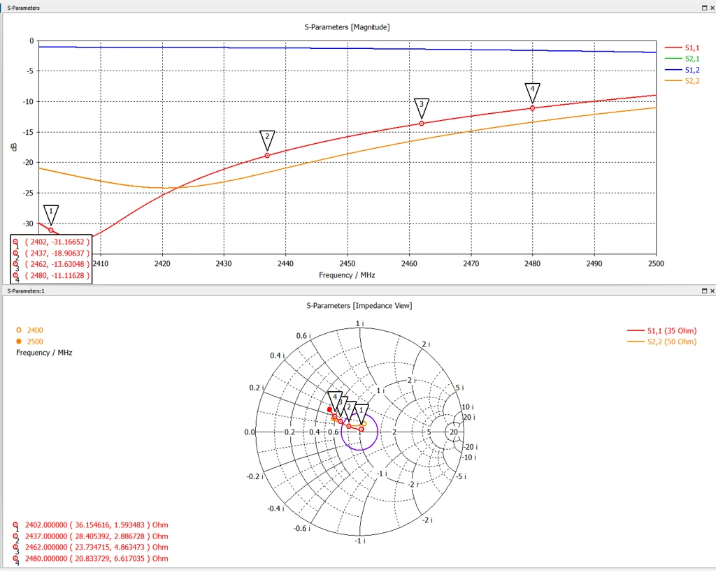
Try a lower capacitance first, if the S1,1 valley moves further from the target channels or the response degrades, try a higher value instead
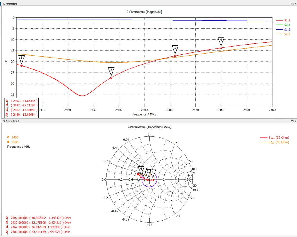
The goal is to position the valley between the four target channel frequencies with the curve staying below the target level at all markers.
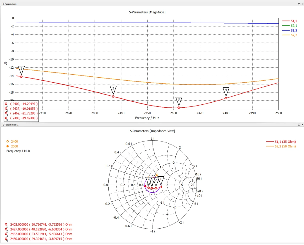
For example: if the initial candidate at 1.5 pF shifts the valley too far toward the lower edge of the band, try 1.4 pF, if that improves the response, try 1.3 pF. If 1.3 pF places the valley too high in the band, try a different variant of the same nominal value, as different package codes and dielectric types within the same capacitance can produce measurably different responses at 2.4 GHz.
Once CRF1 is defined, repeat the entire sequence for R0L and then CRF2, reading the current value from the Block Parameter List, searching SimSurfing, downloading and saving the SPICE model, importing it into the Device Library, applying it to the component, and evaluating the updated combined response. If modifying a later component shifts the response in a way that cannot be corrected within its own value range, return to the previous component and try an adjacent value.
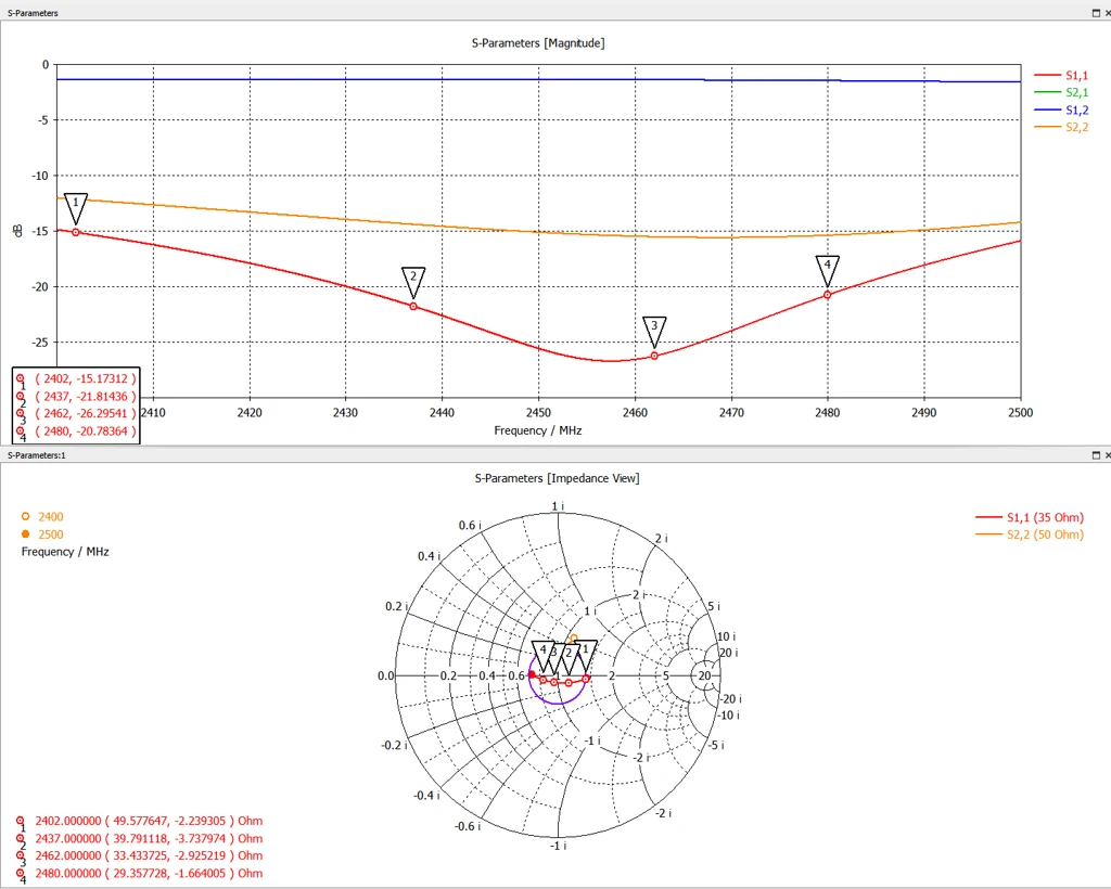
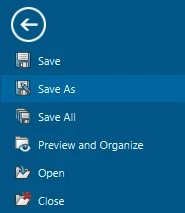
When the response is acceptable, save the project with the suffix _components via File → Save As.

Converting Ports to Lumped Elements for Full 3D Simulation
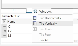
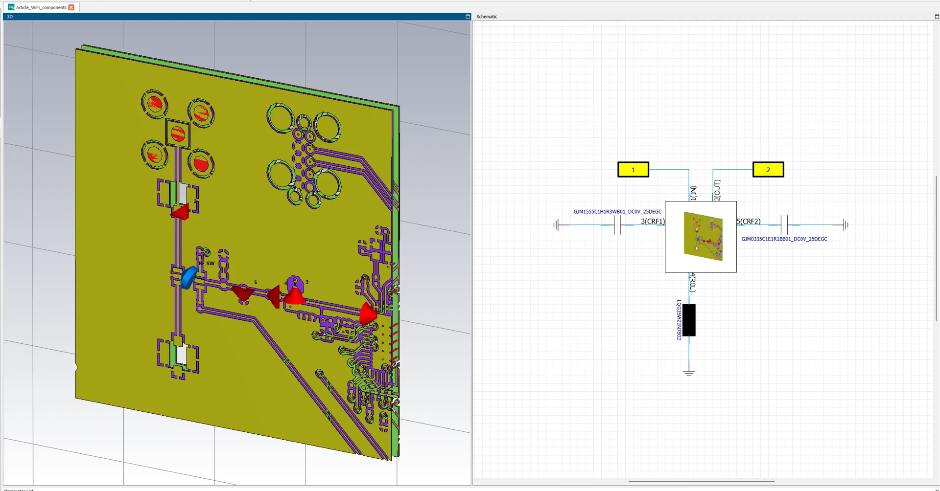
With the component selection complete in the schematic and the project saved as _components, the next step is to transfer the real models into the 3D environment. Close all plot windows and use Tile Vertically to display the 3D view and the Schematic side by side. The part numbers visible on the schematic wires will serve as reference when configuring each Lumped Element, keep them visible throughout this step.
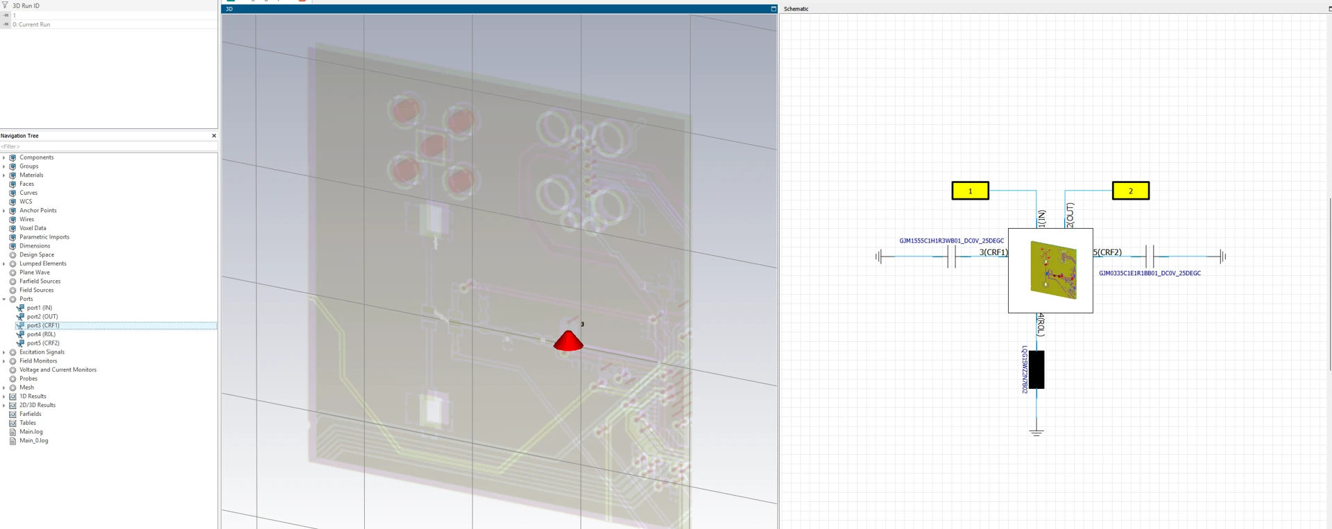
In the 3D view, select the Discrete Port corresponding to CRF1. In the Navigation Tree, the ports are listed under Ports, click port3 (CRF1) to select it and confirm its position in the 3D model.
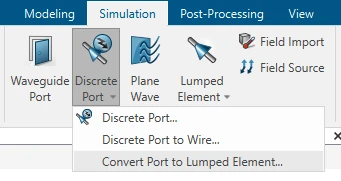
In the Simulation tab, open the Discrete Port dropdown and select Convert Port to Lumped Element.
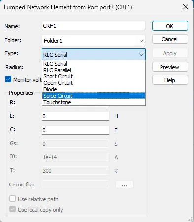
In the Lumped Network Element from Port dialog that appears, set the Name to CRF1. In the Type dropdown, select Spice Circuit.
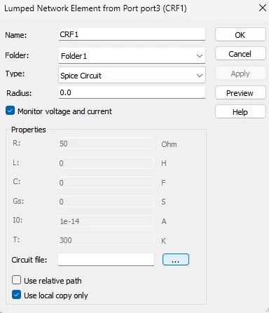
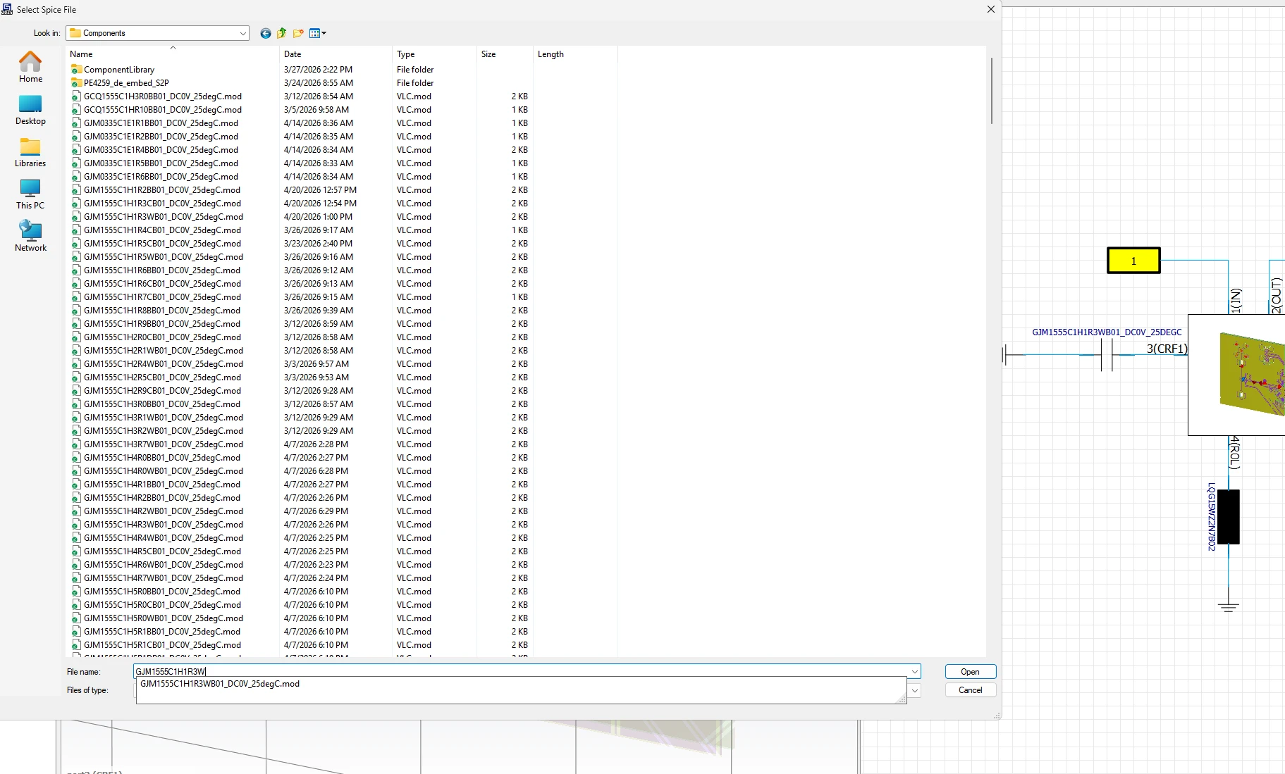
Click the three dots button next to Circuit file. Drag the dialog window aside to expose the Schematic panel and read the part number of CRF1 directly from the schematic wire. Type that name in the File name field, the matching file will appear in the list. Select it and click Open.
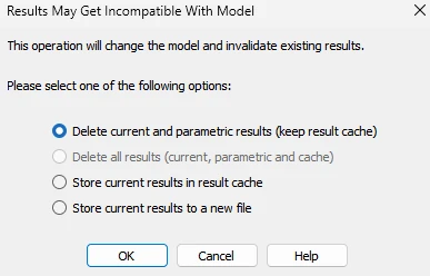
Click OK. A prompt will appear asking whether to delete the existing results, confirm. The Discrete Port marker at the CRF1 position will be replaced by a Lumped Element indicator.
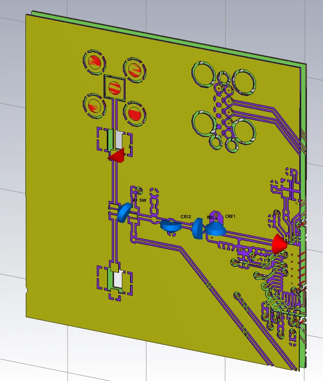
Repeat the same process for R0L and CRF2, reading each part number from the schematic before selecting the corresponding file. When all three ports have been converted, the 3D model will show the Lumped Elements in place of the previous port markers, blue indicators at each component position along the RF path.
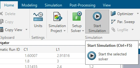
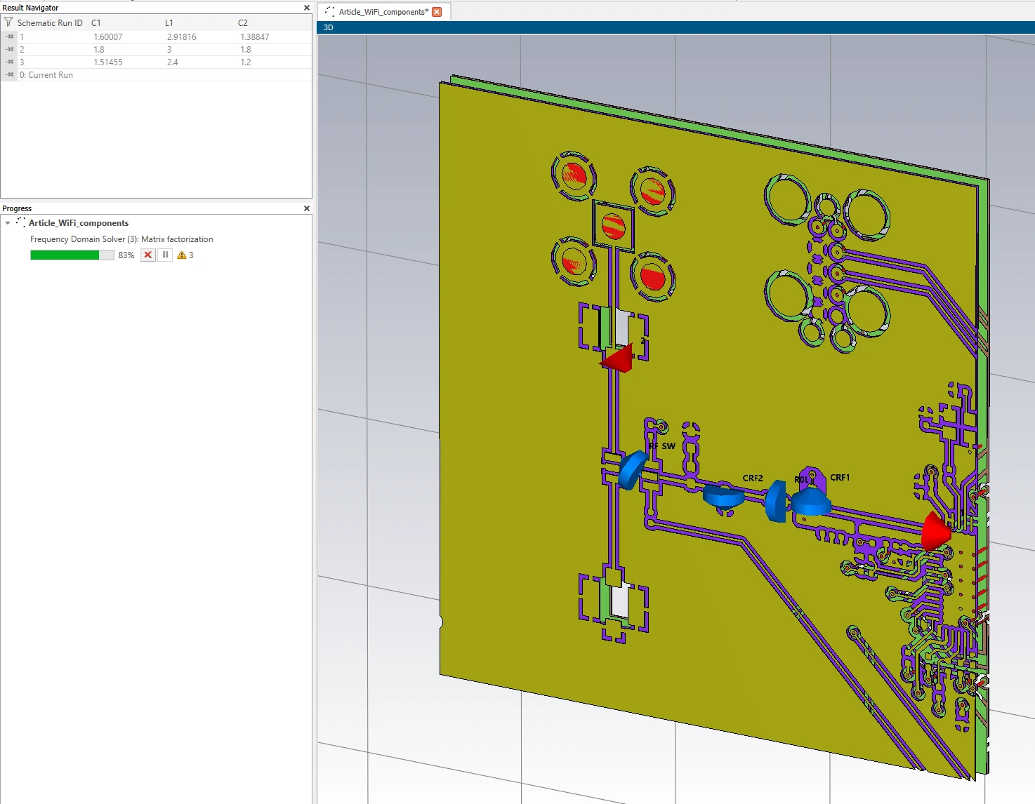
Go to Home → Start Simulation to launch the full 3D electromagnetic simulation. This run is significantly longer than the schematic co-simulation updates performed during component selection, as the solver now computes the complete field distribution across the board volume with the real component models embedded in the structure.
3D Field Results
When the simulation completes, navigate to 1D Results → S-Parameters in the Navigation Tree to verify the final S1,1 response with the real components embedded in the 3D model.
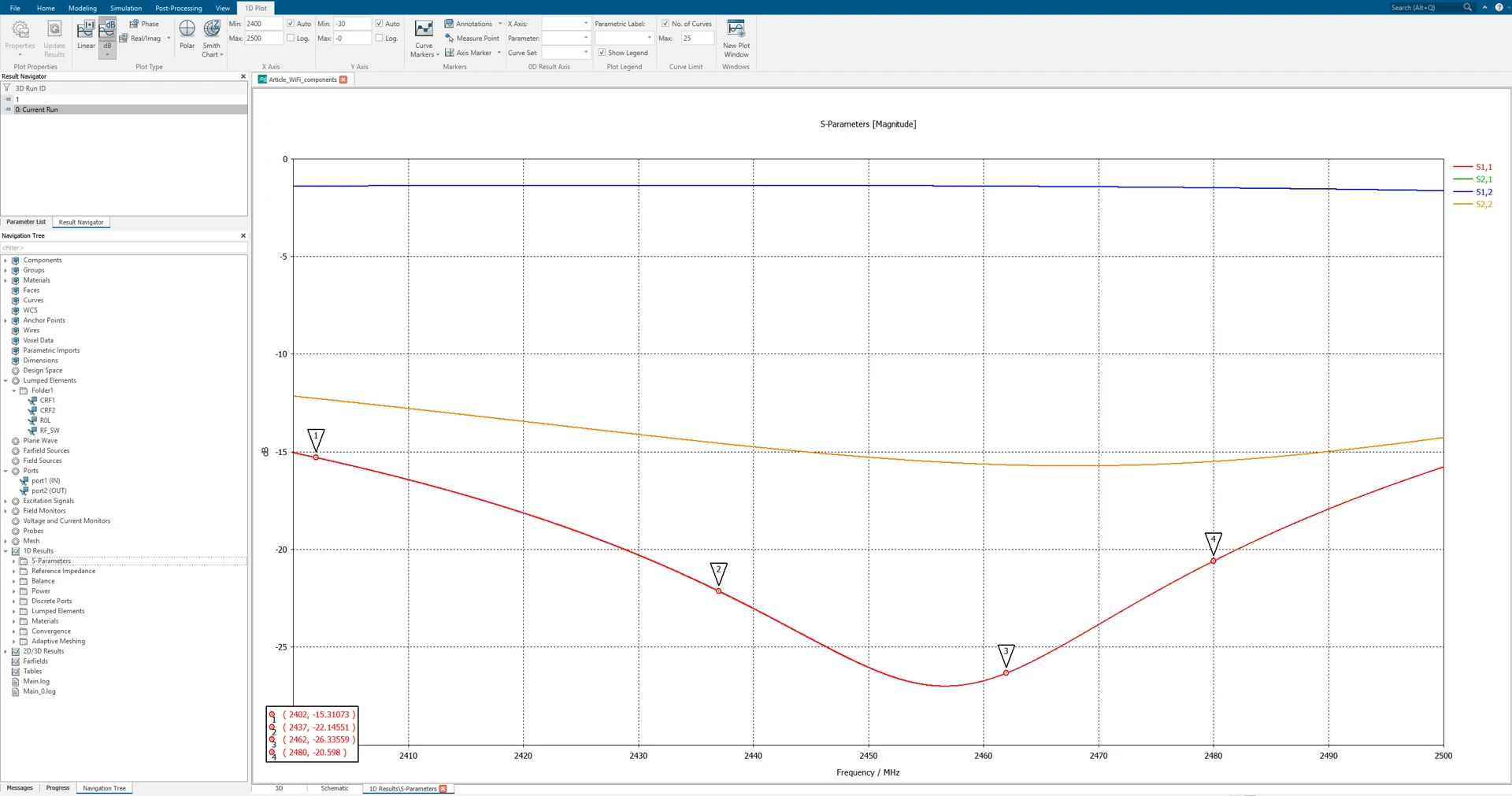
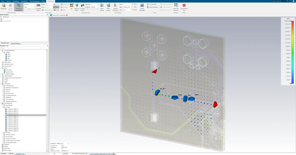
To examine the field distribution, open 2D/3D Results → E-Field in the Navigation Tree and select one of the target frequencies. The default view shows the field as arrows, informative but visually dense when the full board is displayed.
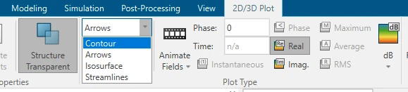
In the 2D/3D Plot tab, change the Plot Type from Arrows to Contour.
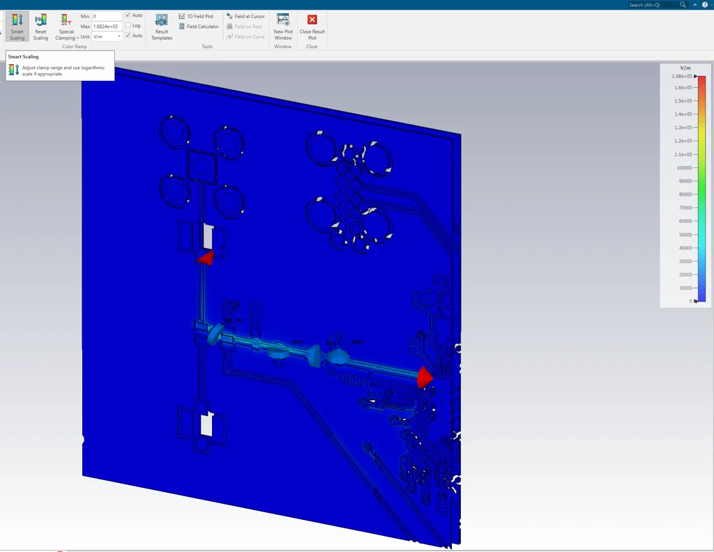
Then click Smart Scaling to allow CST to adjust the color ramp dynamically based on the actual field values in the model. The difference in readability is significant, the Contour representation with Smart Scaling makes the field concentration along the RF trace and around the filter components immediately visible against the low-field regions of the surrounding board.
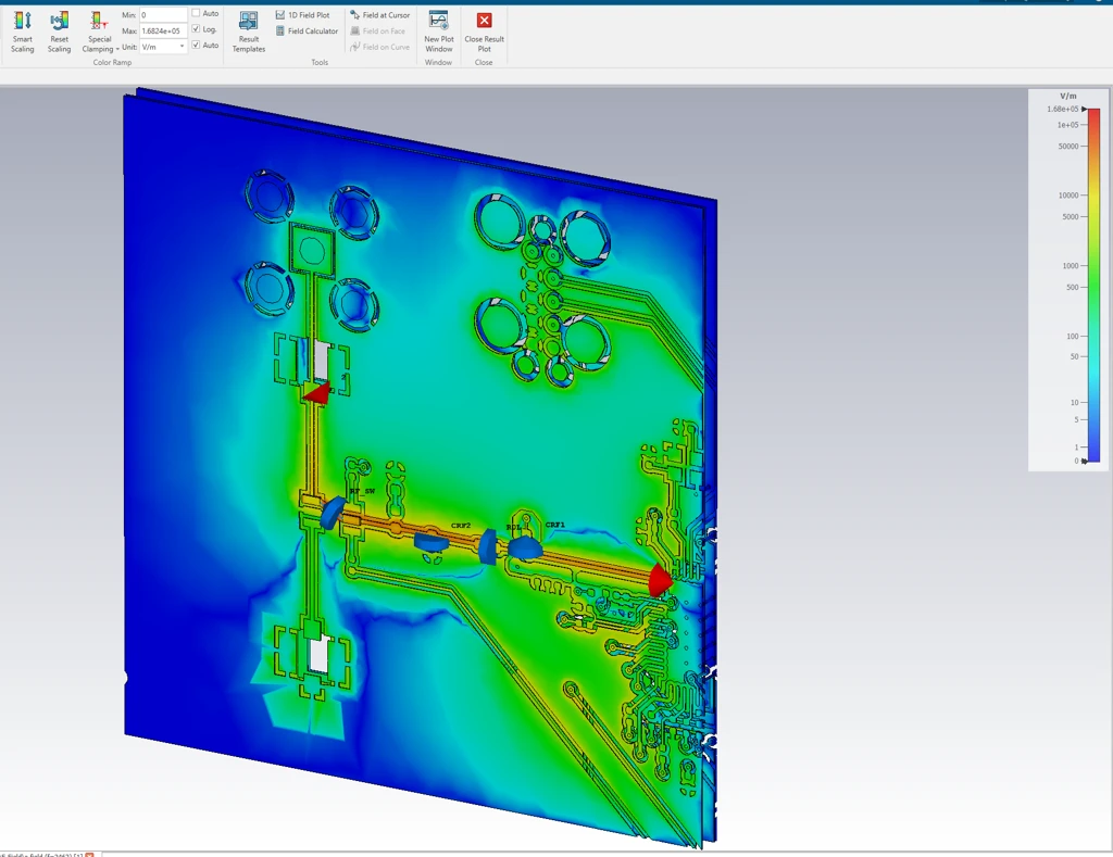
Use the same Contour and Smart Scaling settings when examining the remaining field results in the Navigation Tree: H-Field, Surface Current, Power Flow, and Power Loss Density. Each result reveals a different aspect of the electromagnetic behavior of the board at the operating frequencies. The surface current distribution identifies the high current density regions on the ground plane and the RF traces. The H-field distribution reveals potential magnetic coupling paths around R0L. The power loss density map identifies where the finite Q of the real components and the resistivity of the copper are having the greatest impact on filter efficiency. Together these results define the starting point for the EMI analysis in the next article series.
Update in Altium
With the component selection finalized in CST, the last step of this stage is to update the Altium schematic with the real part numbers determined through the simulation process.
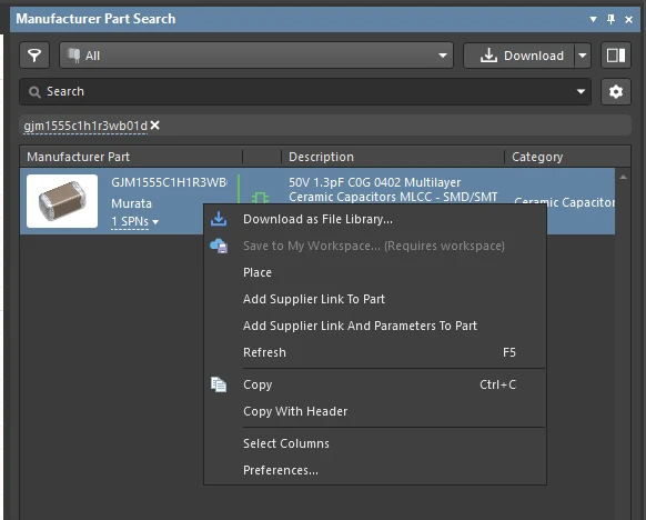
Open the ESP32-S3 schematic in Altium Designer. Open the Manufacturer Part Search panel. Using the part numbers visible in the CST schematic as reference, search for each component by name, for example, gjm1555c1h1r3wb01d for CRF1. The component will typically appear in the search results with its full description, package, and supplier information.
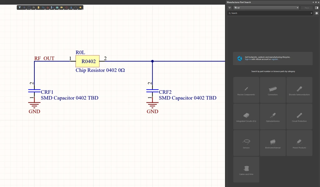
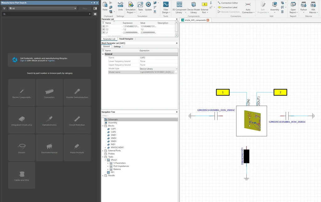
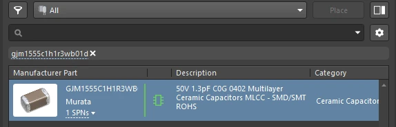
Right-click the search result and select Place to place the new component on the schematic. Position it near the existing placeholder component, assign it the same reference designator, and delete the old component. The schematic will now show the real Murata part number in place of the generic placeholder.
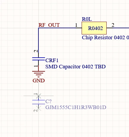
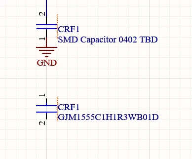
Repeat for R0L and CRF2. When all three components have been replaced, the schematic will show the complete filter network with real, manufacturable parts.
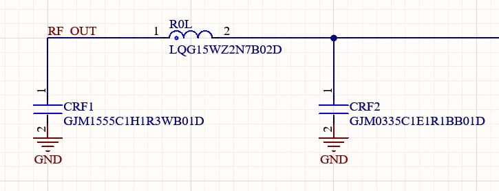
Synchronize the schematic changes to the PCB file to propagate the updated component information to the layout. The PCB is now ready for the EMI analysis stage.
Closing
This third stage completed the convergence from ideal model to physical reality. The filter now exists as a fully characterized electromagnetic structure: its component values are anchored to real Murata parts with known frequency-dependent behavior, validated through an iterative schematic-level selection process before being committed to a full 3D simulation.
The three-stage progression is now visible in full. Stage 1 defined what the filter can achieve when the board does not exist and the components are perfect. Stage 2 showed how the physical layout shifts and distorts that response. Stage 3 showed the further effect of finite Q, parasitic resistance, and self-resonance, and demonstrated that commercial components in the 0402 package can still meet the S1,1 target across the four Wi-Fi 2.4 GHz channels when selected with care.
The field results from the full 3D simulation do more than validate the filter response. The E-field distribution along the RF trace, the H-field concentration around R0L, the surface current density on the ground plane, and the power loss map together identify where the electromagnetic behavior of the board deviates from what an ideal structure would produce. These deviations are the input to the next article series, not as abstract design rule violations, but as specific, located, quantified electromagnetic phenomena that targeted mitigation techniques can address.
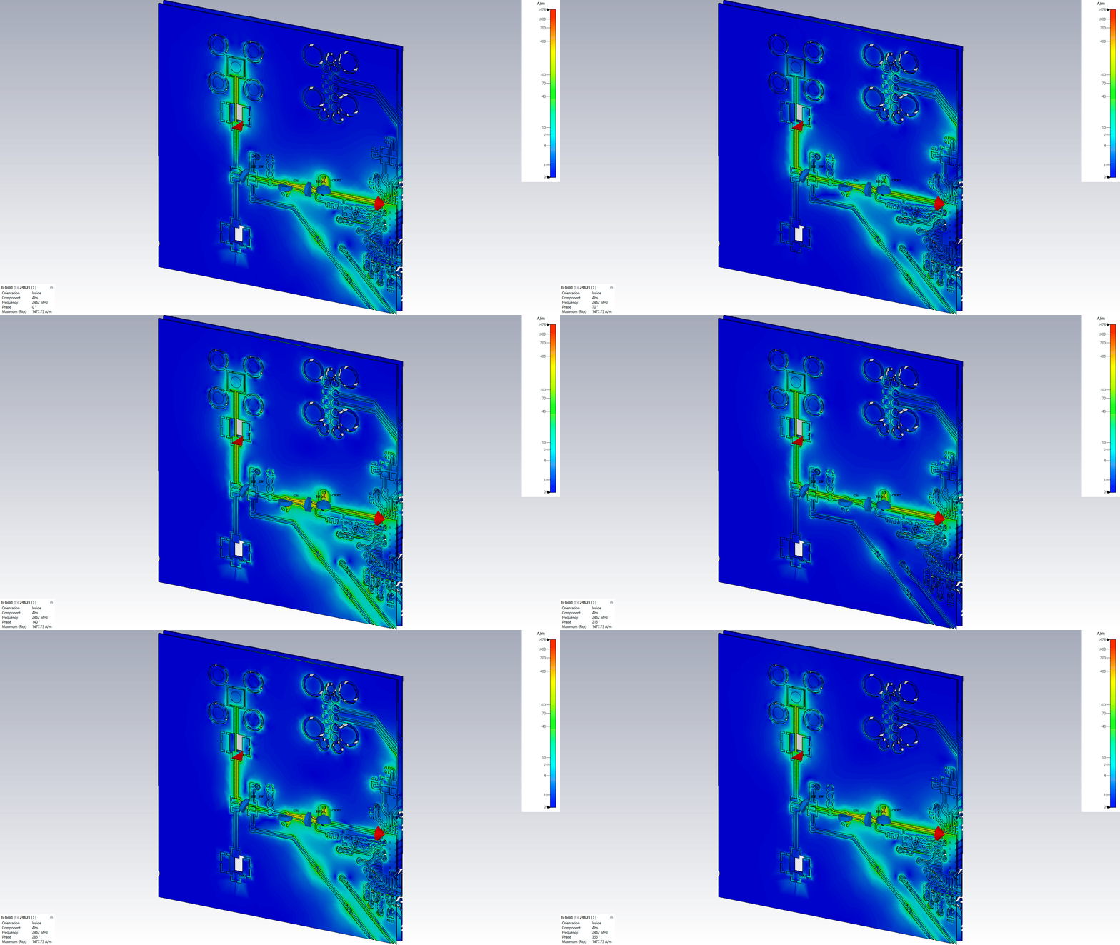
As you can see, the RF signal interferes with other traces, let´s take care of it in the next article.
The Altium schematic now carries real part numbers. The PCB is ready. The next stage begins with the board already understood.